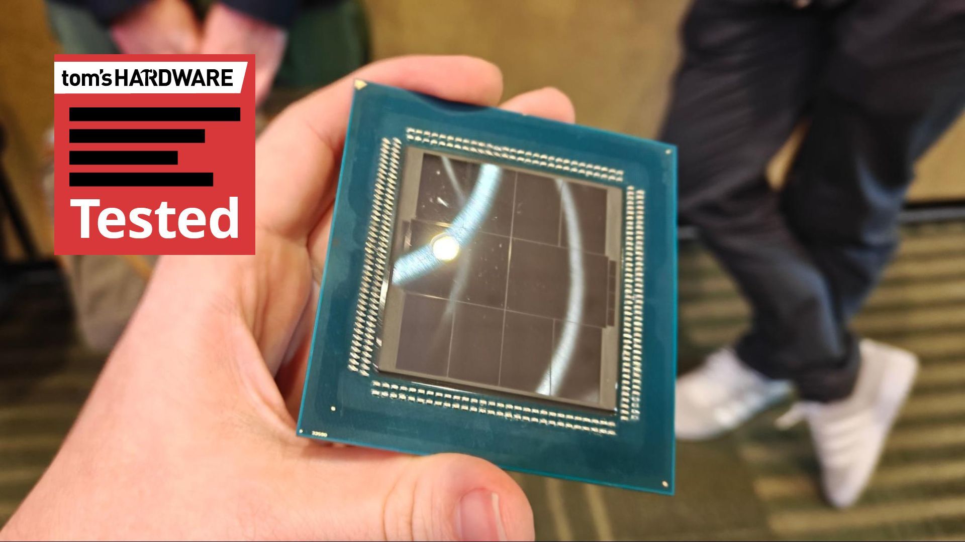
AMD’s EPYC ‘Venice’ CPUs are the first to debut the new Zen 6 architecture, and we’ve been testing two chips from the range over the past several weeks to see how they compare to Nvidia’s Vera, and more broadly, how the Zen 6 architecture departs from Zen 5 ahead of the expected consumer-focused Olympic Ridge launch next year. Zen 5 was a ground-up redesign of AMD’s storied Zen core, and Zen 6 takes that foundation and expands it in just about every regard.
Zen 6 uses TSMC’s N2P node, but it also comes with significant architectural changes under the hood. Within the core, a redesigned vector engine pushes AMD’s SIMD performance even higher, and it now natively supports half-precision FP16 instructions alongside full, 32-bit precision. It also splits integer schedulers within the execution engine, allowing for more instructions in flight through the core.
Across the die, AMD made other significant changes. The single IOD of previous generations is now split across two IODs, giving the SP7 platform access to 16 memory channels (though at the cost of PCIe 6.0 lanes compared to the previous generation and SP8 platform).
The CCDs have been upgraded, too, for the first time since Zen 3. A standard Zen 6 CCD can now scale up to 12 cores, while a Zen 6c packs 32 cores. With Zen 5 and 5c, CCDs topped out at eight cores and 16 cores, respectively. For the Zen 6c CCD, AMD also doubled the amount of shared L3 per core, which effectively quadruples the L3 compared to Zen 5c, since the CCD packs twice the number of cores.
Interestingly, Zen 6 is neither a marginal optimization to Zen 5, nor a complete architecture redesign. Stepping back, it looks like AMD pushes as many dials as it has access to to their highest level, and that holds up looking at performance.
The 256-core EPYC 9996 delivers 1,024 threads in a 2P configuration, which came out 93% ahead of the 768-thread 2P EPYC 9965 server we tested in SPEC CPU 2026’s intrate throughput test. The frequency-optimized EPYC 9686F excels elsewhere, notably in scientific computing and HPC workloads, and it serves as AMD’s competitor to Vera, at least before the LPDDR-based Verano platform arrives from AMD next year.
AMD says it believes Venice is fundamentally a generation ahead of the competition, which would be a worthless line if it wasn’t backed up by data. Intel’s Granite Rapids-AP is rarely in the conversation, and although Vera maintains some competitive positions, Venice is often ahead — sometimes orders of magnitude ahead.
Intel’s Diamond Rapids is set to launch next year, which should help balance the scales. But AMD has set an incredibly high bar with Venice, one that it will likely extend even higher for some workloads with the arrival of Venice-X and Verano next year.
There’s a lot to get to here. We have a full deep dive into the Zen 6 microarchitecture, a broader look at the chip itself, the platform(s) AMD is pushing out this generation, and of course, more than 100 benchmarks covering everything from Python performance to HPC.
AMD Zen 6 microarchitecture breakdown
AMD Zen 6 microarchitecture breakdown
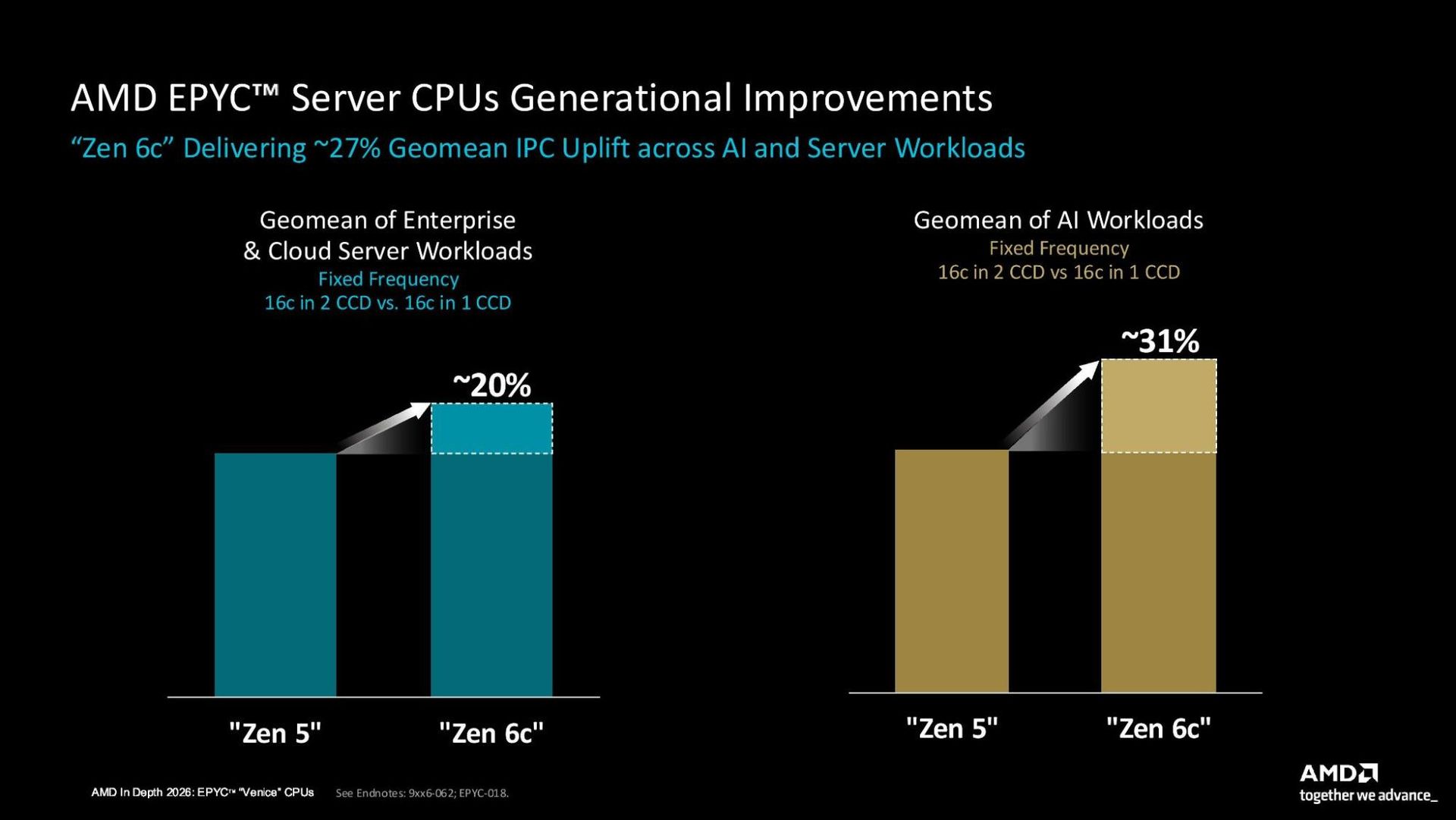
The headline for Zen 6 is a 27% average IPC uplift over Zen 5 in enterprise, cloud, and AI workloads. The debut of this new microarchitecture is focused on the data center, so you shouldn’t take that 27% IPC improvement as broadly applicable to all workloads. Additionally, AMD arrived at that number by comparing fixed-frequency Zen 5 to Zen 6c with 16 cores. As we’ll get into in the next section, a Zen 6c CCD can comfortably fit 16 Zen 6c cores with room to spare, while 16 Zen 5 cores are split across two CCDs.
The compute die is built on TSMC’s N2P node, which is an already optimized version of N2 that comes with a 5% performance improvement. Compared to N3E (Zen 5 used N4P), N2P offers an 18% speed improvement at iso-power, or a 36% reduction in power at the same speed.
Speed Improvement (v. N3E) | Power Improvement (v. N3E) | Density (v. N3E) | |
TSMC N2P | +18% (iso-power) | -36% (iso-speed) | +15% |
AMD described Zen 5 as a ground-up redesign when the microarchitecture first broke cover in mid-2024, characterized by a wider execution engine capable of dispatching and returning eight instructions per cycle, a wider frontend to feed it, full AVX-512 support, and doubled bandwidth between the L2 and L1 cache. Zen 6 is a continuation of the redesign we saw on Zen 5. It carries many of the same characteristics, as well as the same general topology, just enhanced in a number of ways.
As we go through the breakdown, keep in mind that Zen 6 and Zen 6c use the same microarchitecture. Zen 6c is just a space-optimized design that consumes less power, clocks lower, and, obviously, takes up less die space than a full Zen 6 core. But, the company uses the same microarchitecture inside the core, unlike Intel’s E-cores, which use a different microarchitecture than the P-cores.
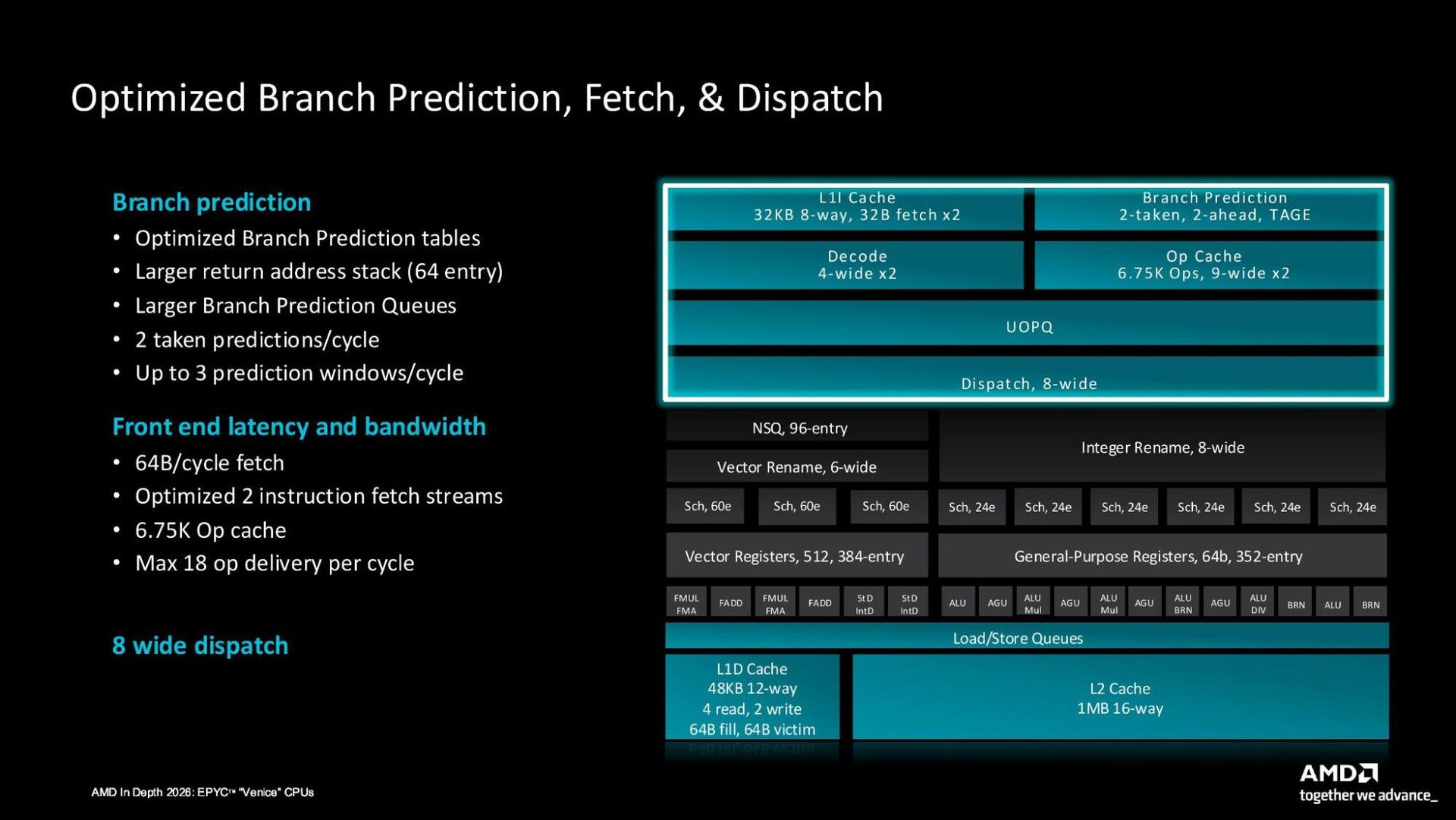
Starting with the frontend, it’s largely unchanged from Zen 5, short of a few notable improvements. You get the same dual 4-wide decode pipes and 8-dispatch, but AMD has improved the BPU and op cache. For the BPU, it has a 64-entry Return Address Stack, up from 52 on Zen 5. AMD also increased the op cache size back up to 6.75K entries from 6K on Zen 5 (Zen 4 also had a 6.75K-entry op cache). This larger cache can serve up to 18 micro-ops per cycle, up from 12 on Zen 5.
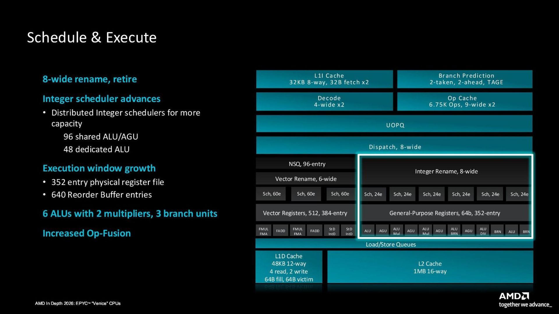
AMD split the integer schedulers for Zen 6 (Zen 5 had a unified scheduler), now offering higher capacity, with 96 shared ALU/AGU and 48 dedicated ALU entries, compared to an 88 / 56 split for ALU/AGU on Zen 5. AMD also expanded the general-purpose registers to a 352-entry physical register file, up from 240 on Zen 5.
The vector execution engine is also improved, following on the heels of a true 512-bit register in Zen 5. Zen 6 carries forward that 512-bit data path and adds some additional improvements. Notably, the engine now supports half-precision AVX-512 FP16 instructions, which needed to be converted in Zen 5’s vector execution engine. Also notable is the FP load/store bandwidth. Zen 5 supports two loads of any size, but Zen 6 supports either two 512-bit loads or four 256-bit loads. Store bandwidth is unchanged, at one 512-bit store or two 256-bit stores.
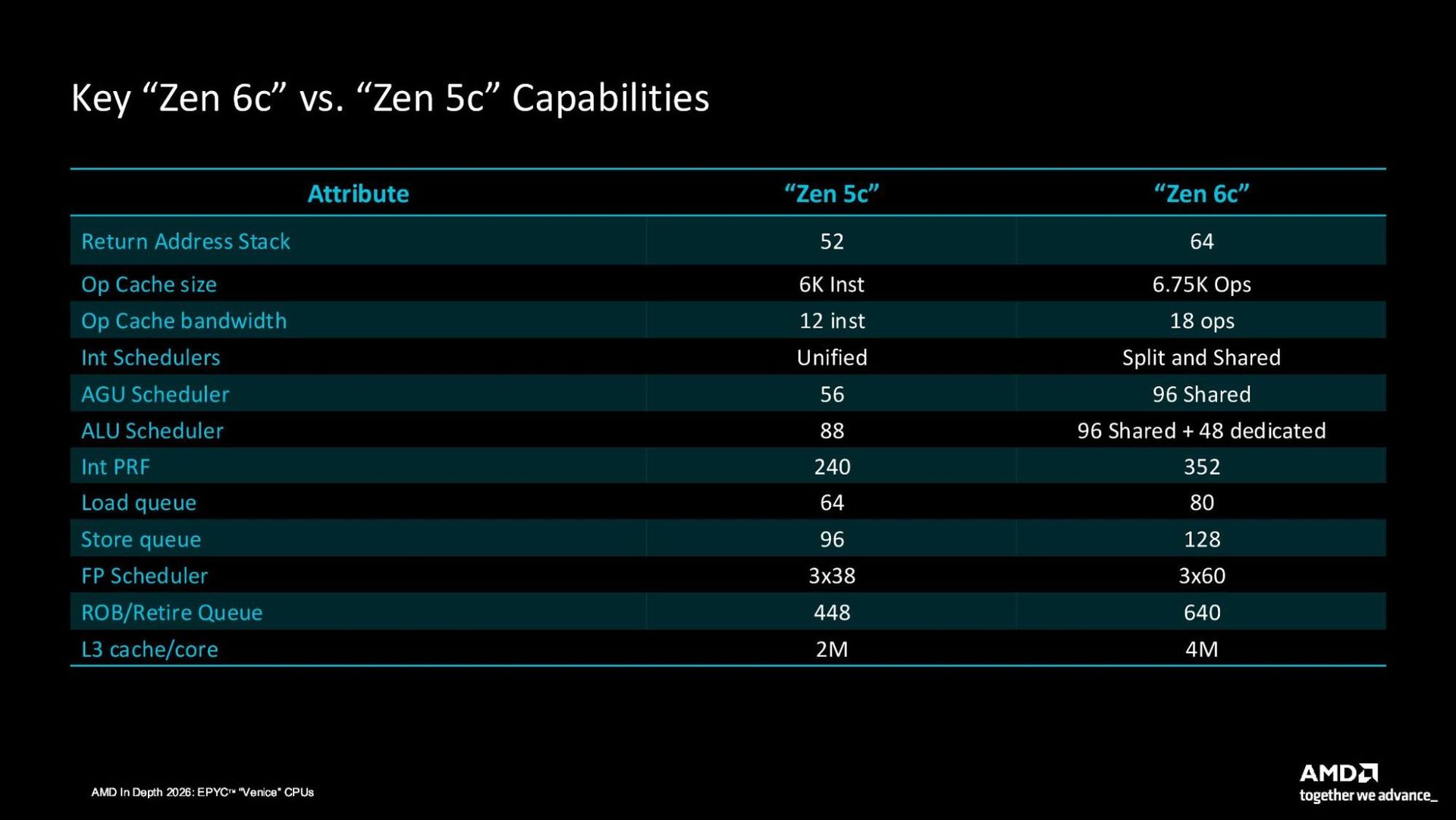
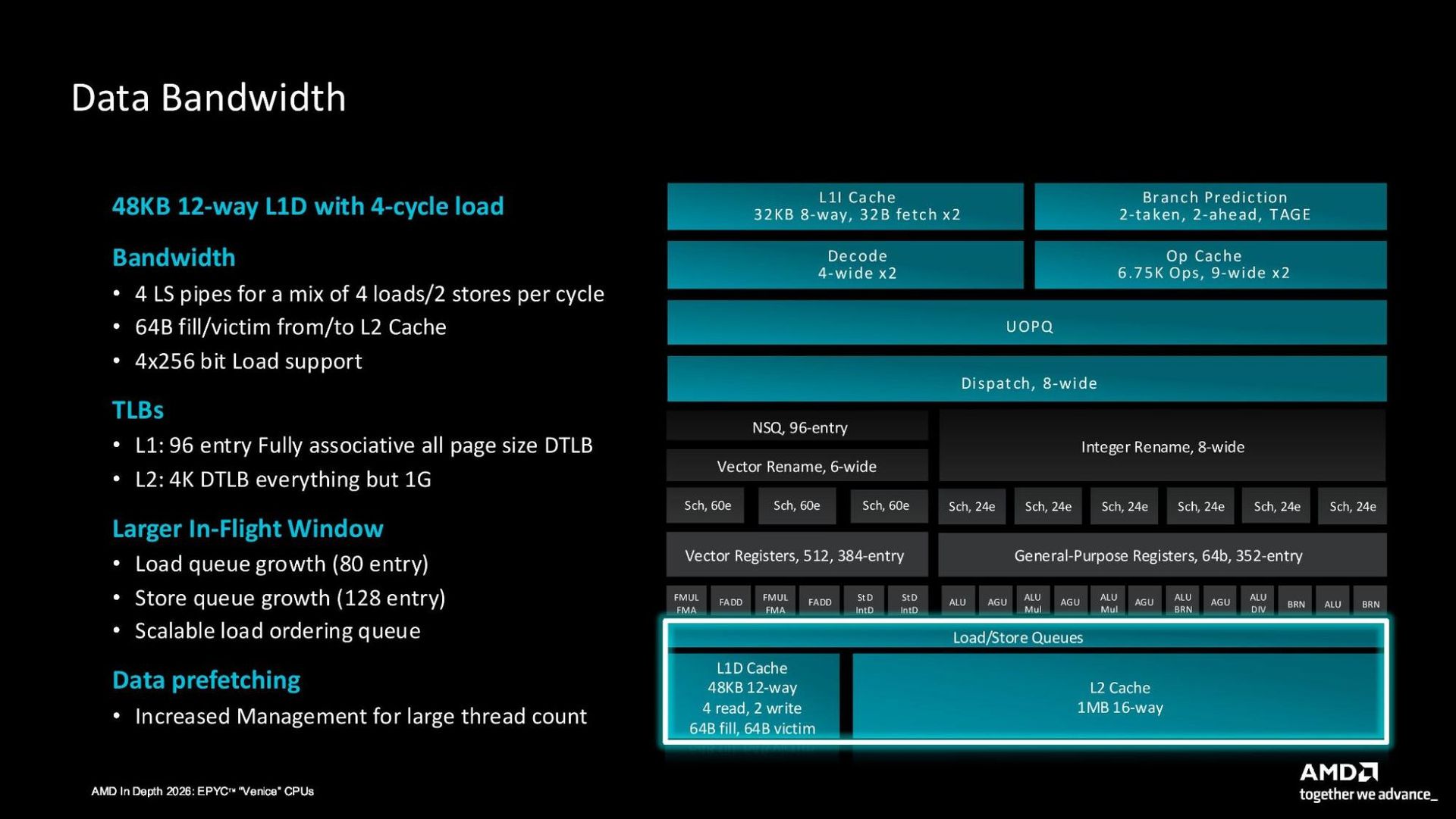
Zen 6 carries forward the 48 KB 12-way L1 data cache from Zen 5, along with 1 MB 16-way private L2. The shared L3 is treated as victim cache for the L2, as is the case in Zen 5. However, AMD increased the in-flight window compared to Zen 5, with an 80-entry load queue and 128-entry store queue.
AMD Zen 6 and Zen 6c CCD and platform breakdown
AMD Zen 6 and Zen 6c CCD and platform breakdown
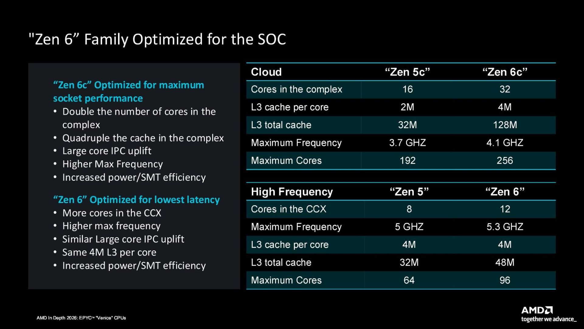
Perhaps the biggest change going from Zen 5 to Zen 6 comes in the density of the CCD. Zen 6 offers up to 12 cores per CCD, up from 8 on Zen 5, while Zen 6c scales up to 32, double that of Zen 5c. Elsewhere, the updated CCDs either match or improve on Zen 5/5c CCDs.
For Zen 6, AMD retained the 4 MB of L3 cache per core, increasing the total cache to 48 MB to accommodate the new 12-core limit. The maximum frequency of a standard Zen 6 CCD has increased from 5 GHz on Zen 5 to 5.3 GHz on Zen 6. Keep in mind these clocks are in the context of Venice; we expect higher maximum boost clocks on consumer Olympic Ridge.
Zen 6c has more enhancements. AMD doubled the amount of L3 per core from 2 MB to 4 MB, matching the normal Zen 6 CCD. And, with double the L3 per core and double the number of cores, the Zen 6c CCD has a total of 128 MB of L3, quadruple that of a Zen 5c CCD. For Zen 6c, the maximum frequency is also up, going from 3.7 GHz on Zen 5c to 4.1 GHz on Zen 6c.
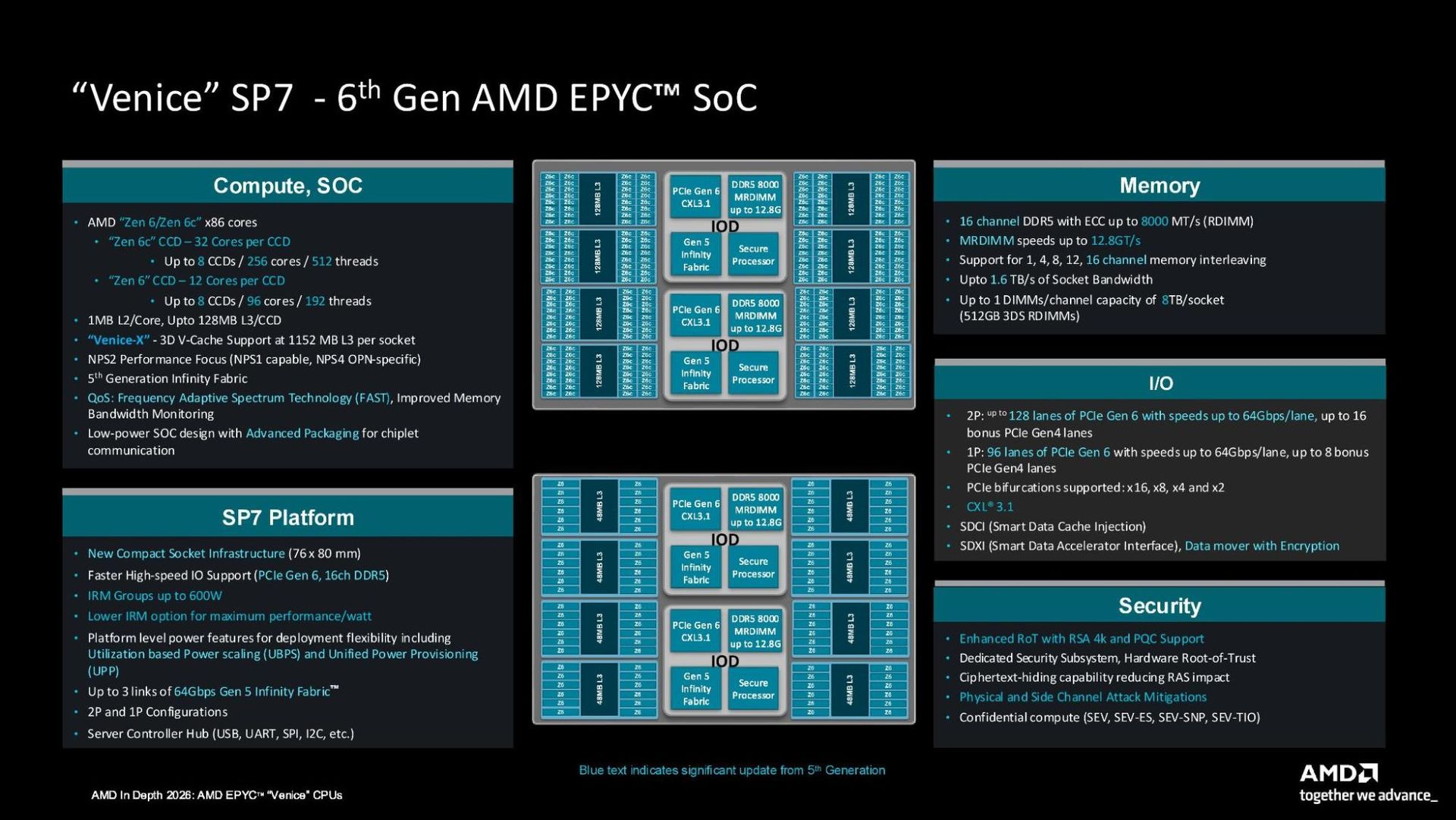
Across both, AMD claims a “large core IPC uplift,” as well as improved power and SMT efficiency. We haven’t seen an overall IPC claim yet, though the numbers referenced above put Venice at about a 27% advantage over Turin in enterprise, cloud, and AI workloads.
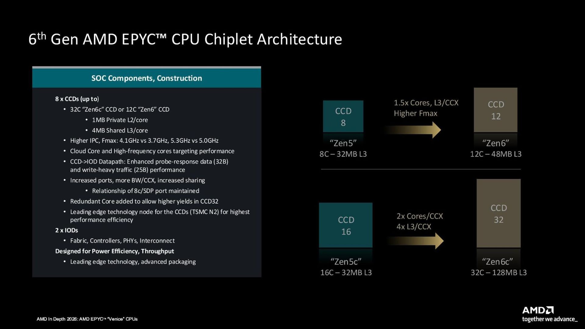
In the context of Venice, AMD can fit up to eight CCDs on a chip, coming out to 256 cores in total for Zen 6c, and 96 cores total for regular Zen 6 for SP7 platforms (the initial lineup for Venice). AMD is moving past the SP5 socket available to Genoa and Turin CPUs for SP7, which is a slightly larger socket at 76 x 80 mm (SP5 is ~72 x 75 mm).
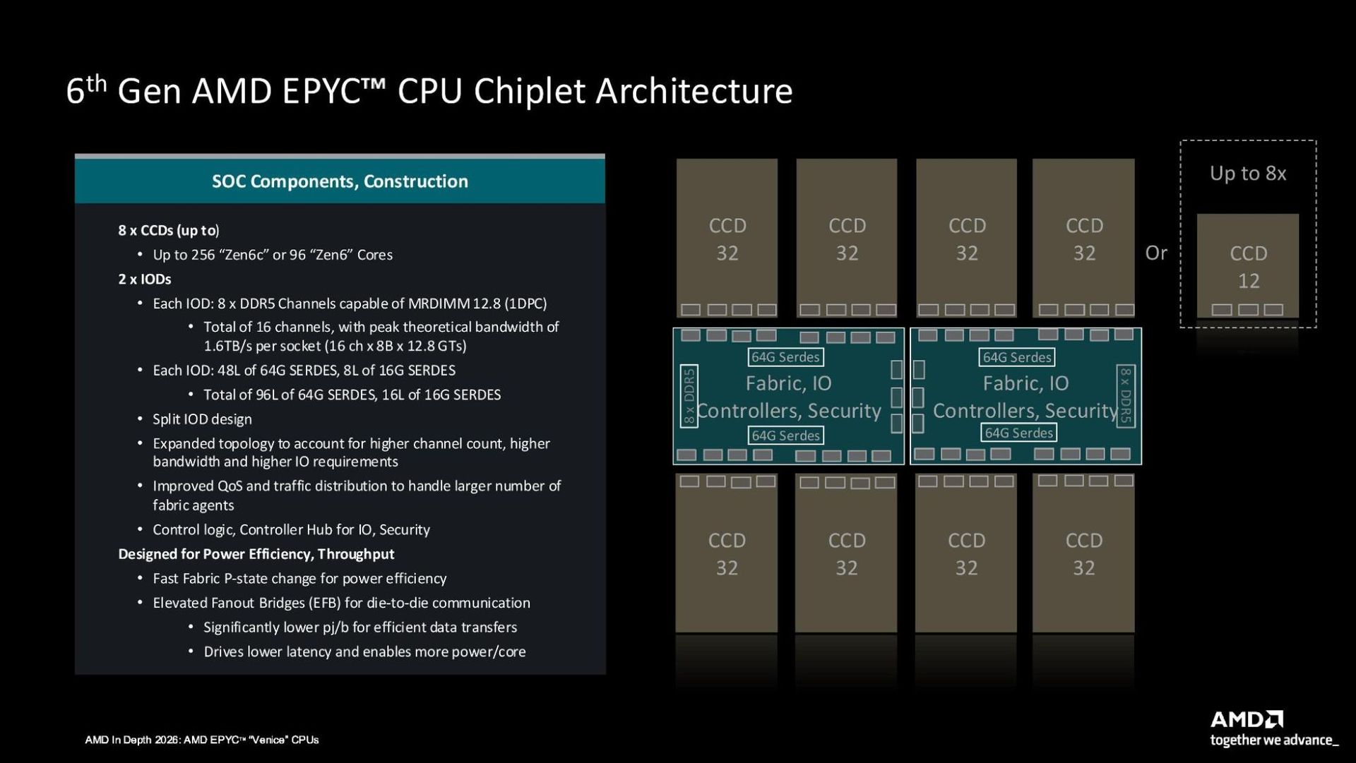
The topology of the chip is largely intact from Turin, short of the dual IO dies that characterize Venice. The two IODs live in the middle of the chip, flanked by Zen 6 CCDs. The second IOD is what gives SP7 chips access to 16 channels of memory per socket (8 channels per IOD), supporting up to 12,800 MT/s speeds using MRDIMMs in a 1DPC configuration. With RDIMMs, AMD supports up to 8,000 MT/s. The platform supports up to 8 TB of memory per socket, and AMD claims bandwidth of up to 1.6 TB/s per socket (1 TB/s per socket with RDIMMs).
Also on the IOD, there’s the hardware root-of-trust, as well as AMD’s confidential computing extensions, including execution encryption, memory integrity, and trusted I/O. New to the platform is PCIe 6.0 at speeds up to 64 Gbps per lane. A 1P SP7 configuration has access to 96 PCIe 6.0 lanes, while a 2P platform has up to 128. Each configuration also comes with “bonus” PCIe 4.0 lanes, either 8 for 1P configs or 16 for 2P.
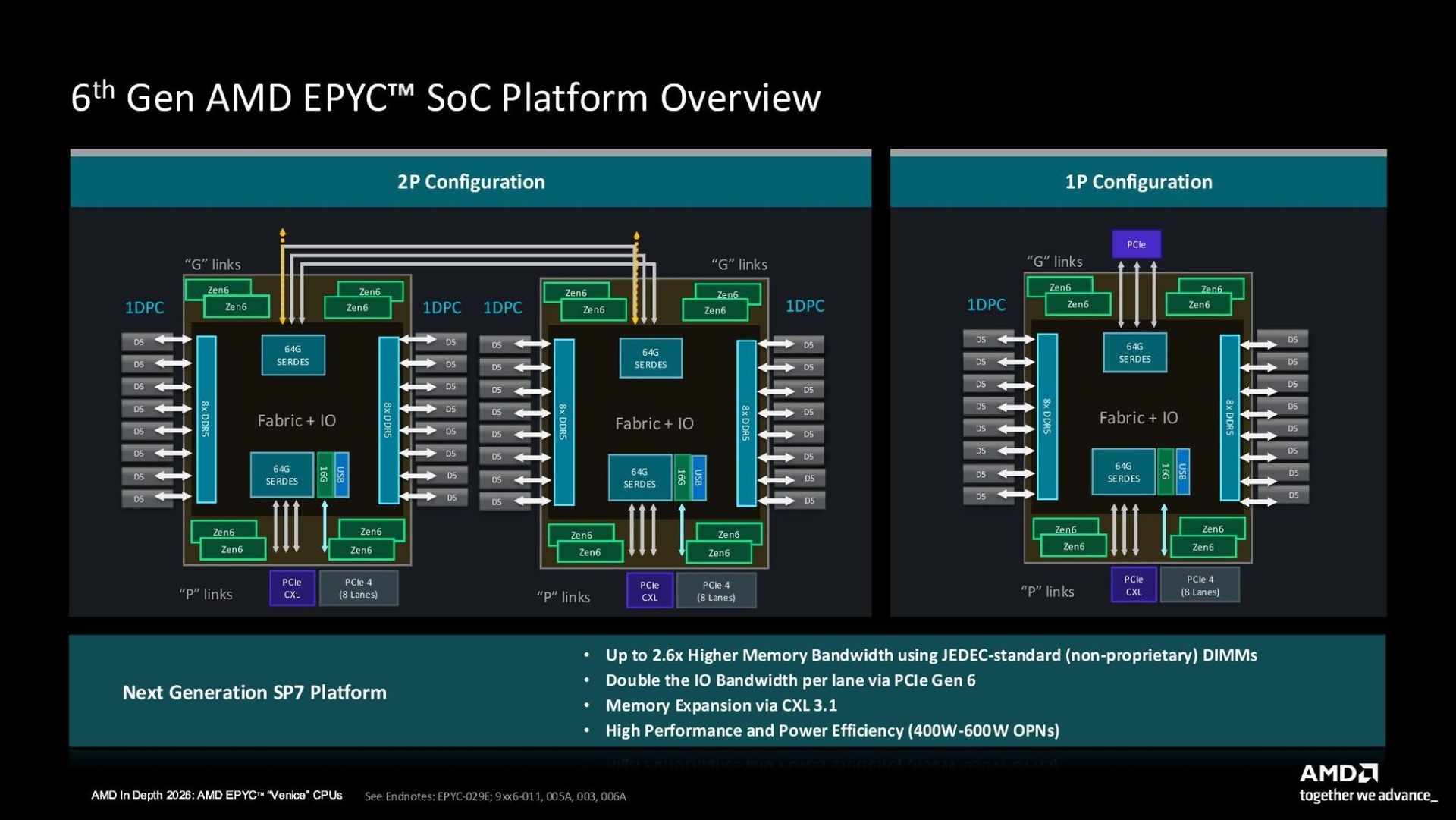
Two 64G SerDes interfaces bring the PCIe lanes into the IOD, one of which is used to link the chips in a 2P configuration. That second interface can still optionally handle an additional 12 PCIe 6.0 lanes, giving the “up to” 128 2P lanes number. The bonus lanes run through a smaller 16G SerDes interface.
Platforms with the SP8 socket trade memory channels for PCIe lanes. The SP8 socket is smaller at 62.5 x 80 mm, and the platform supports eight memory channels instead of 16, though with the same support for up to 12,800 MT/s MRDIMMs. Memory bandwidth drops to 819 GB/s for MRDIMMs and 512 GB/s for RDIMMs at the maximum supported transfer rate.
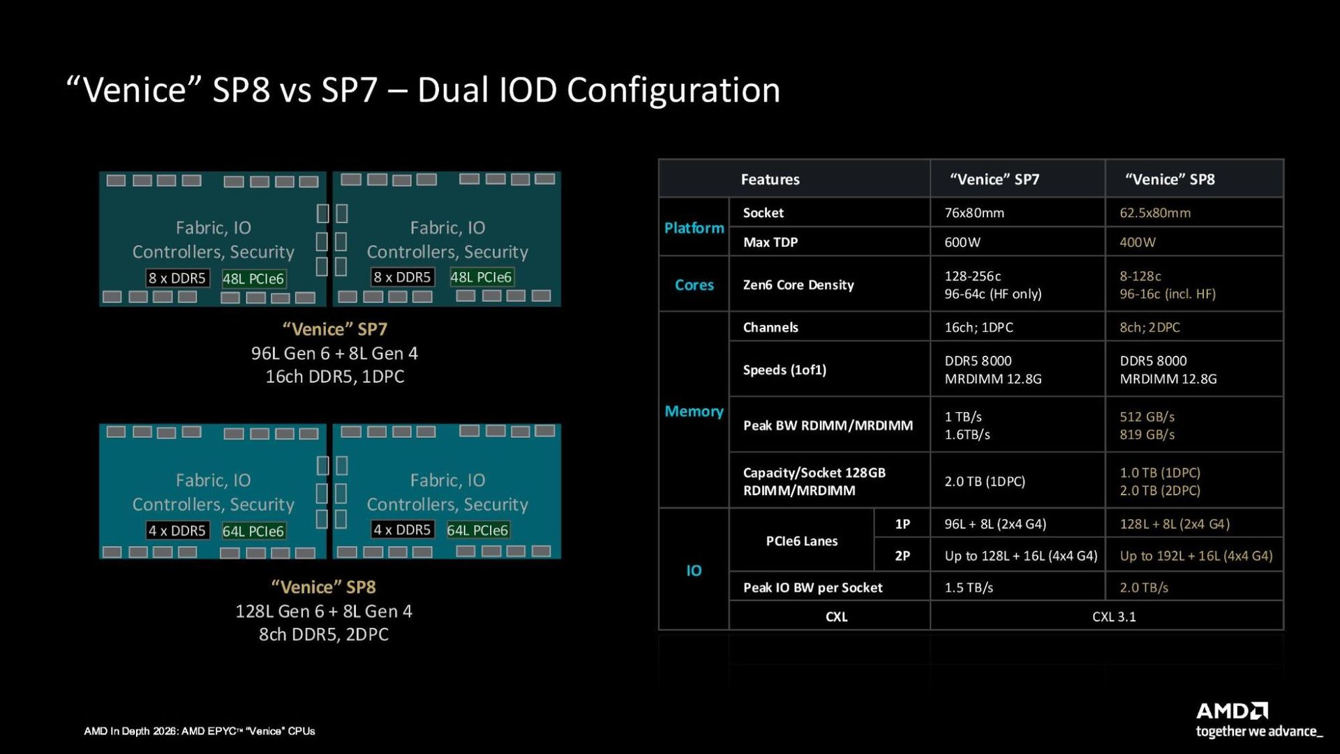
However, SP8 chips have access to 64 PCIe 6.0 lanes per IOD, for a total of 128 lanes in a socket (plus the additional eight PCIe 4.0 bonus lanes). Just like SP7, some of those lanes are shared in a 2P configuration, dropping the total to 192 PCIe 6.0 lanes in 2P SP8 servers, with 16 additional PCIe 4.0 lanes. Both platforms support CXL 3.1.
AMD also provided a platform breakdown for its upcoming Verano range, which uses the Zen 6 microarchitecture on an LPDDR5X-based platform, leveraging replaceable SOCAMM2 DIMMs.
UPP, UBPS, and FAST in Zen 6 ‘Venice’ CPUs
UPP, UBPS, and FAST in Zen 6 ‘Venice’ CPUs
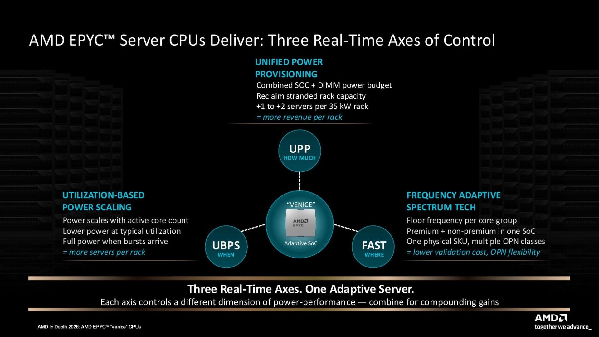
AMD has added a few quality-of-life features to Venice CPUs that should make them easier to manage when actually deployed. First is UPP, or Unified Power Provisioning, which is a power management feature that takes into account total platform power, allocating it as needed to different components, depending on the workload. With it, AMD says it’s able to deliver a power consumption of 830W on 16 servers to 706W on 18 servers, or a decrease in provisioned power by 15%, while increasing the number of servers per rack.
Also dealing with power is UBPS, or Utilization Based Power Scaling. It’s a dynamic power scaling feature that aligns with whatever workload is running on the server, which AMD says “helps close the gap between provisioned and consumed power.” Like UPP, UBPS is concerned with platform power, not just the power consumption of the CPU.
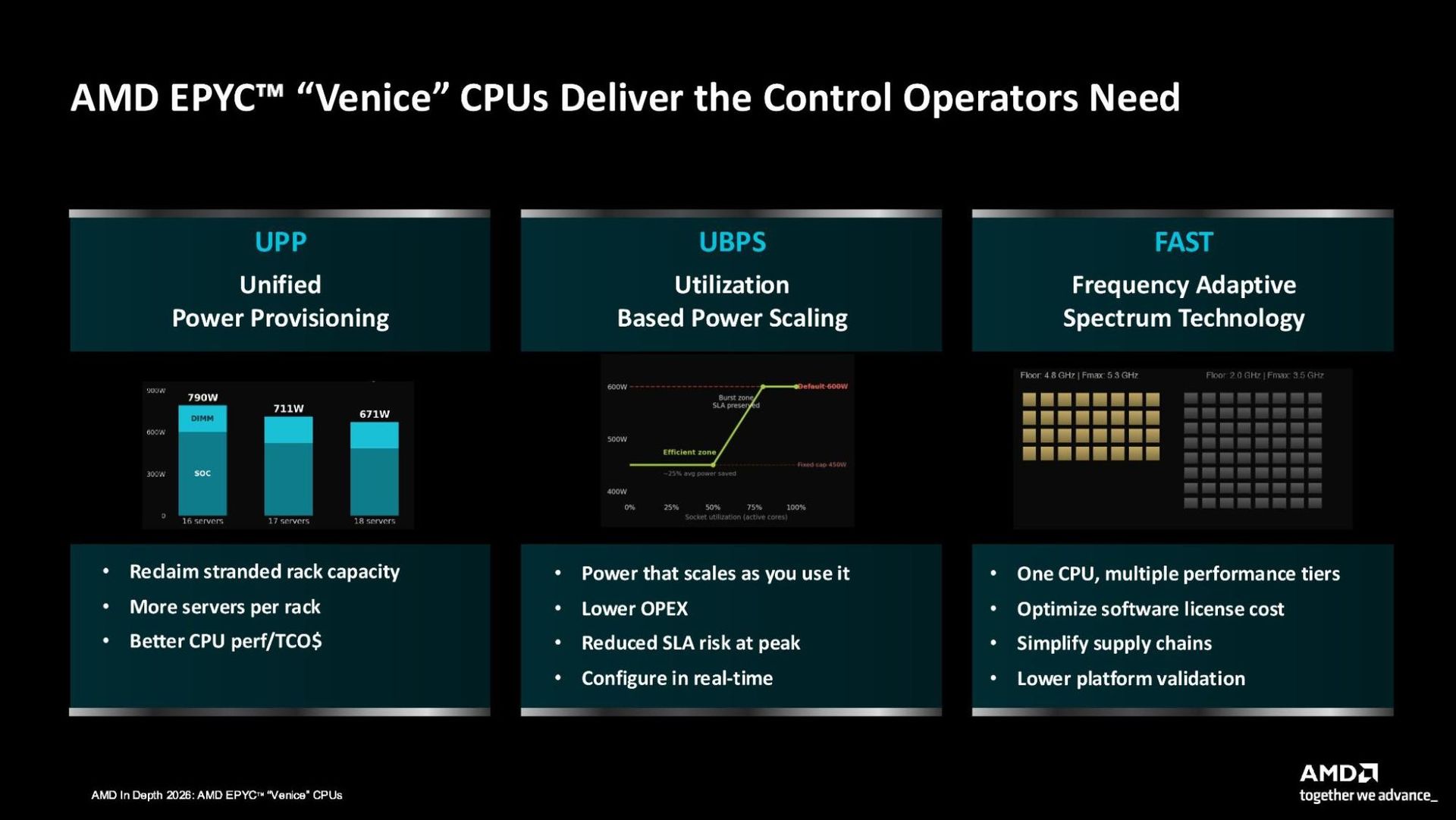
The most interesting addition is FAST, or Frequency Adaptive Spectrum Technology. The feature takes in telemetry from the platform and policies set in firmware to adjust the frequency within set power and thermal limits. It sounds a little more involved than a simple Precision Boost Overdrive for the data center, however.
AMD described FAST to us as allowing for two performance tiers within one socket. As an example, AMD pointed to a 96-core Venice CPU, saying FAST allows 32 of those cores to run in a “premium” category, with a base clock of 3.65 GHz and a max clock of 5 GHz, while a “batch” category with 64 cores runs at 2 GHz with a 2.4 GHz max. AMD described it as multiple commercial SKUs within a single socket.
Preliminary MEXT support, claims of 95% performance at 50% DRAM capacity
Preliminary MEXT support, claims of 95% performance at 50% DRAM capacity
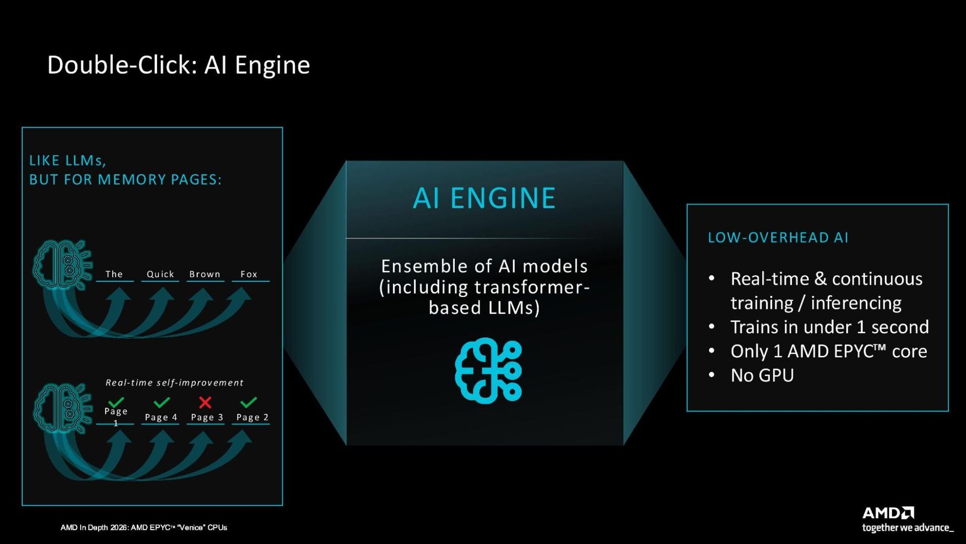
Venice marks the point when AMD will start offering MEXT on its EPYC platforms. AMD aquired MEXT earlier this year, and it has used the feature internally. With HPE, AMD is rolling out “MEXT ready” platforms, which will, eventually, have access to MEXT licenses. The technology is interesting, especially given how constrained memory is right now.
The general concept of MEXT is using flash as DRAM. Even the fastest flash is orders of magnitude slower than DRAM, but MEXT attempts to take advantage of DRAM access patterns to expose more memory to the system without it actually being there. Pages that haven’t been accessed in several minutes are offloaded to flash storage, and an AI model predicts pages that are needed. Then, those pages are loaded back into memory as you need them.
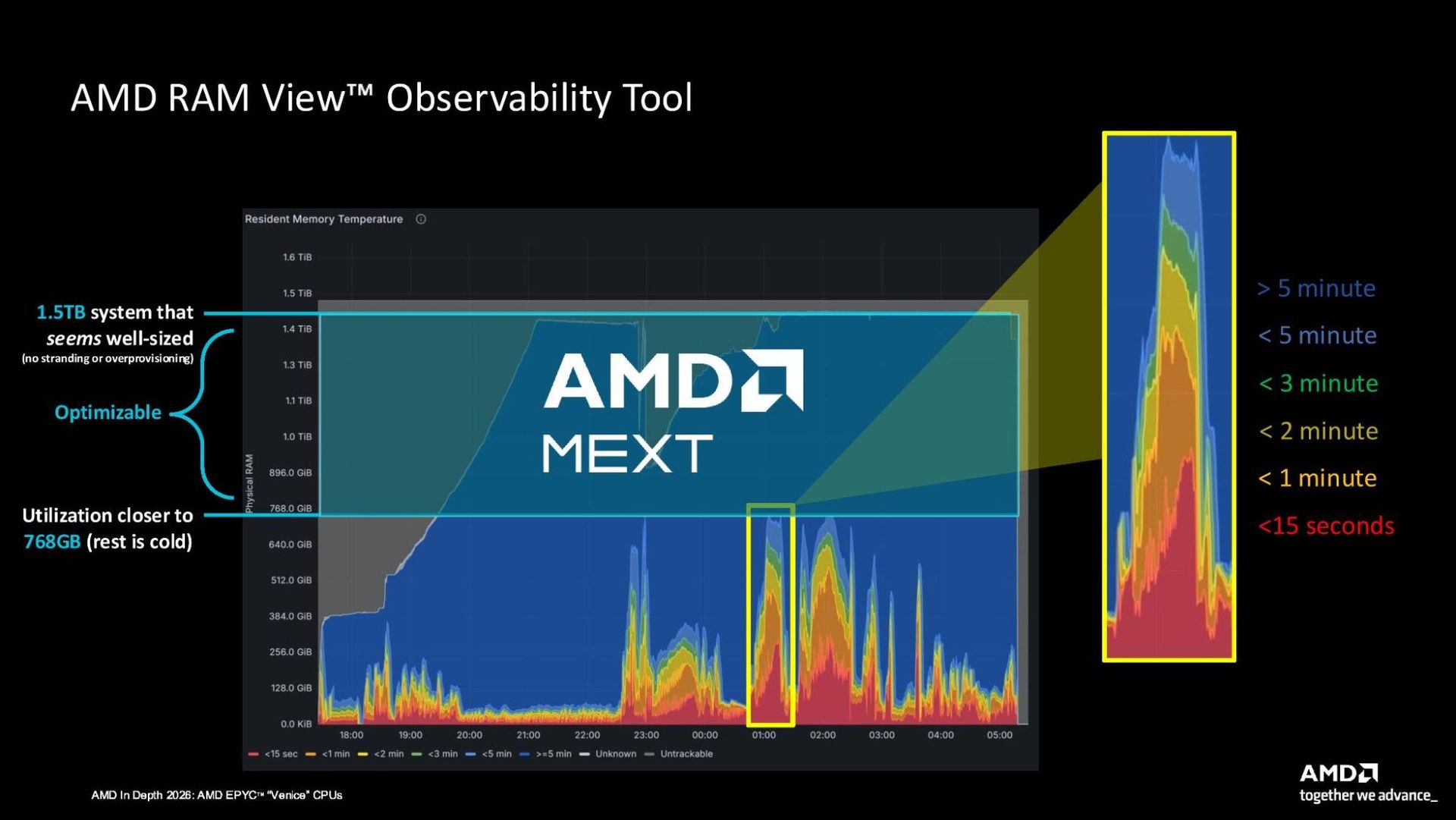
Conceptually, it sounds too good to be true. AMD pointed out that MEXT is using a transformer-based LLM, and effectively, LLMs are predicting what words go next when generating text. Here, AMD says the bar isn’t even that high. As long as the model can stream the correct pages in, and do so fast enough to cover the flash latency, the order of them doesn’t matter.
MEXT is delivered through a Linux kernel module, and AMD has bold claims about its capabilities. The company has deployed the software internally on 145 servers, which it expects to expand to over 2,000 servers next year. Currently, AMD is using it for critical EDA workflows, such as Synopsis PrimeTime. The company says that it’s able to maintain 95% of the application’s performance on Venice with just 50% of the system DRAM. Going down as low as 25%, the company claims the app maintains 80% of its performance.
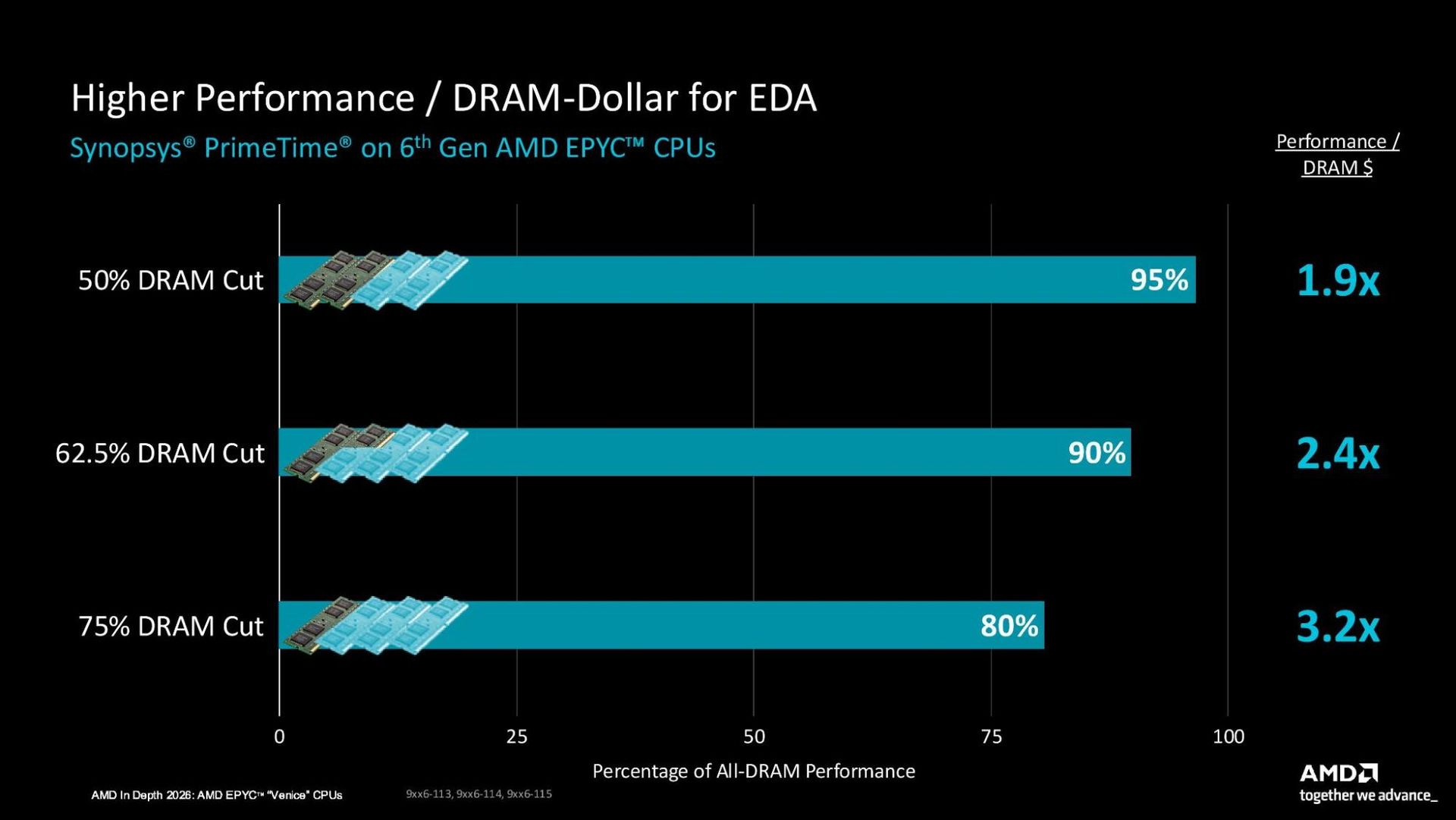
We’ll have more on MEXT shortly. The feature is exclusive to EPYC CPUs, and AMD was clear that it only applies to certain workloads right now. There are likely applications where you won’t be able to cut the DRAM capacity of a server, or where you’ll need to use a more conservative cut of 25% or less.
AMD Zen 6 EPYC ‘Venice’ test configurations
AMD Zen 6 EPYC ‘Venice’ test configurations
AMD gave us access to two Zen 6 Venice systems for the purpose of testing, both of which were dual-socket servers. For the first system, we tested the dense EPYC 9996, which is AMD’s high-core-count design, packing 256 cores and 512 threads per socket, for a total of 512 cores and 1024 threads across a 2P system. It’s a peak throughput SKU, designed to handle heavily concurrent workloads.
On the other end of the spectrum, we have the EPYC 9686F, which is still a high core count CPU in its own right, with 96 cores and 192 threads, giving a 2P system 192 cores and 384 threads. The “F” suffix for AMD’s data center CPUs notes a high-frequency SKU, designed to push performance up in more demanding applications, as opposed to the dense, frontend-focused EPYC 9996.
Chip | Cores / Threads | Base / Boost Clock (GHz) | L3 Cache | TDP |
Epyc 9996 | 256 / 512 | 2.55 / 4.1 | 1024 MB | 600W |
Epyc 9966 | 192 / 384 | 2.9 / 4 | 768 MB | 600W |
Epyc 9846 | 168 / 336 | 2.85 / 3.7 | 768 MB | 500W |
Epyc 9756 | 128 / 256 | 3.15 / 4 | 512 MB | 500W |
Epyc 9G76 | 96 / 192 | 3.4 / 4.8 | 384 MB | 500W |
Epyc 9656 | 96 / 192 | 3.05 / 3.7 | 512 MB | 400W |
Epyc 9686F | 96 / 192 | 3.4 / 5 | 384 MB | 500W |
Epyc 9556 | 64 / 128 | 2.75 / 4.3 | 384 MB | 300W |
Epyc 9586F | 64 / 128 | 3.75 / 5 | 384 MB | 500W |
Both chips use AMD’s SP7 socket, which is geared toward data centers, with higher core count SKUs. The upcoming SP8 socket is focused on enterprise customers, with smaller core counts and support for fewer memory channels.
Although the EPYC 9996 is a dense design with the Zen 6c core, it comes with a fairly high boost clock of 4.1 GHz, though a much lower 2.55 GHz base clock, which it will likely be running closer to in real deployments. It comes with a massive 1,024 MB pool of L3 for the chip, as well as a 600W rated TDP, though it can be manually adjusted between 400W and 600W.
The EPYC 9686F proves out AMD’s claims about Venice, serving as one of two chips in the SP7 lineup to boost up to 5 GHz. It has a lower 500W TDP, though it can again run between 400W and 600W. This is the SKU AMD has heavily referenced in its published Venice benchmarks as a “96-core HF” model.
It’s an interesting model, perhaps more so than the EPYC 9996. It’s in direct competition with Nvidia’s Vera CPU, not only based on core count, but also on performance. These two chips trade blows in several benchmarks, and it’s clear that AMD is pushing this SKU as its “agentic CPU” of the Venice lineup, similar to how Nvidia has positioned Vera.
Test Platform | Memory | Tested Processors |
2P AMD Nigeria reference platform | 32 x 64 GB (2TB) SK hynix DDR5-12800 ECC MRDIMM | AMD EPYC 9996, EPYC 9686F |
2P AMD Volcano reference platform | 24 x 64 GB (1.5 TB) SK hynix DDR5-6000 ECC RDIMM | AMD EPYC 9965, EPYC 9755 |
2P Supermicro SYS-222HA | 24 x 64GB (1.5 TB) Micron DDR5-8800 ECC MRDIMM | Intel Xeon 6980P |
2P Nvidia MGX Vera reference platform | 16 x 96 GB (1.5 TB) Samsung LPDDR5-9600 ECC SOCAMM2 | Nvidia Vera |
You can see the platforms we tested above. The Nigeria reference platform we tested these Zen 6 chips on came with top-end DDR5-12800 MRDIMMs, arranged to fully saturate the 16-channel memory with 32 sticks. This massive jump in memory support is a critical aspect of Venice, particularly for the hotly contested EPYC 9686F and its all-important matchup against Vera.
Vera’s use of LPDDR5 SOCAMM2 memory allows for higher transfer rates than standard RDIMMs in a field-replaceable package, though through a relatively tame eight-channel setup. Vera can get away with 8-channel memory, however, with its topology allowing for massive data movement across the chip. AMD’s distributed design necessitates a bigger memory configuration, with double the channels and access to even higher transfer rates through the use of MRDIMMs.
AMD Zen 6 EPYC ‘Venice’ 9996 and 9686F SPEC estimates
AMD Zen 6 EPYC ‘Venice’ 9996 and 9686F SPEC estimates
Starting off our benchmarks is SPEC CPU 2026, the de facto industry benchmark for server CPU performance. As usual with SPEC runs, the numbers below are “estimates.” We gathered the numbers from real SPEC runs, but we haven’t reported them to the SPEC committee, so they remain “estimates.”
For the throughput benchmark suites, intrate and fprate, we ran a number of copies for each application equal to the thread count of the chip. All of our tests were run on Ubuntu Server 26.04 with Linux Kernel 7.0, and we used GCC 15.2 for all but the Venice chips. GCC 16 brings official support for Zen 6, which we used here. However, we did regression testing against GCC 15 and found only minor differences, and nothing that would change our standings.
Using GCC 16 was important to keep our optimization flags equal. We used common GCC flags, including fast link-time optimization and march/mcpu flags to expose the correct processor instruction support. We also used the open-source jemalloc memory allocator across all tested systems.
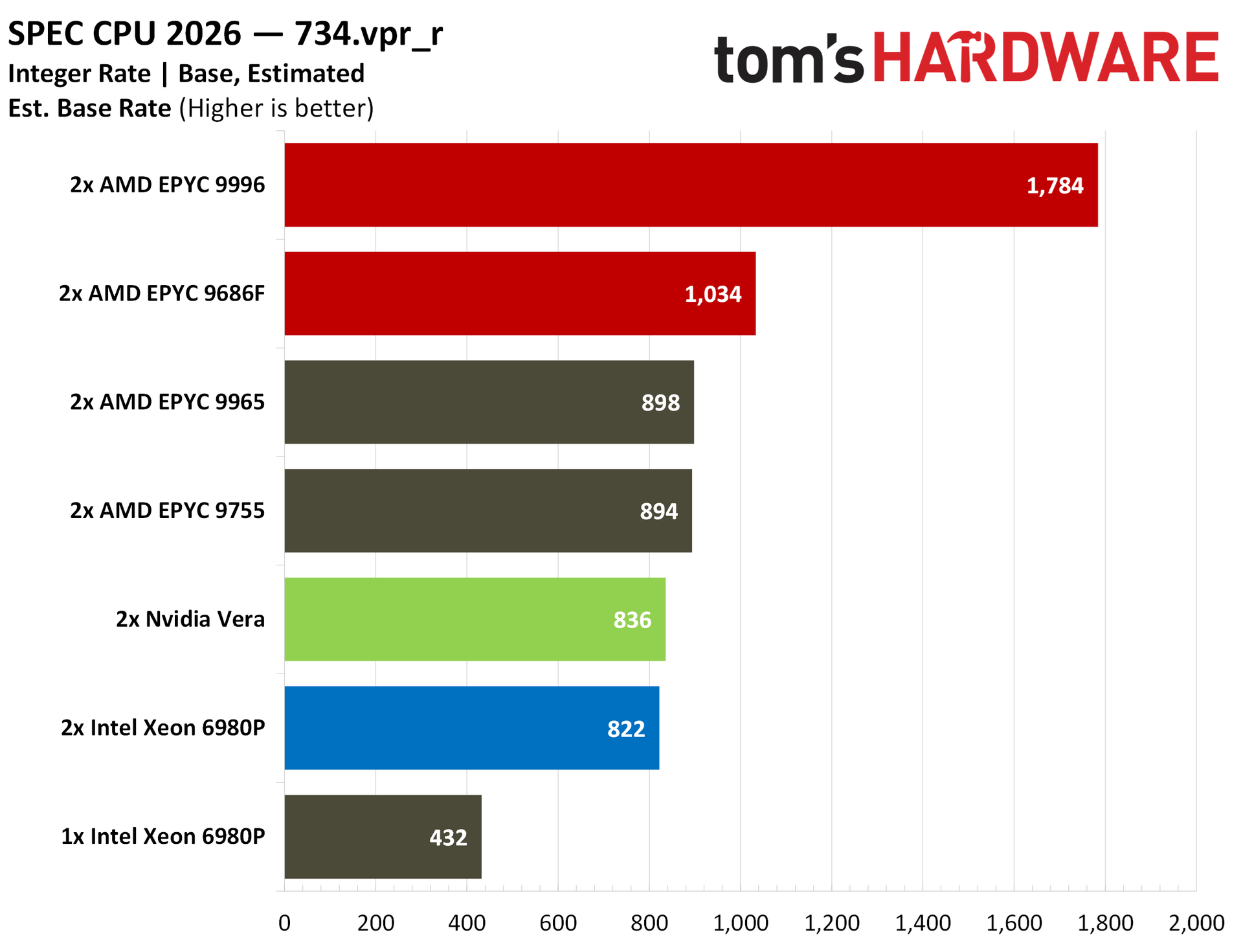
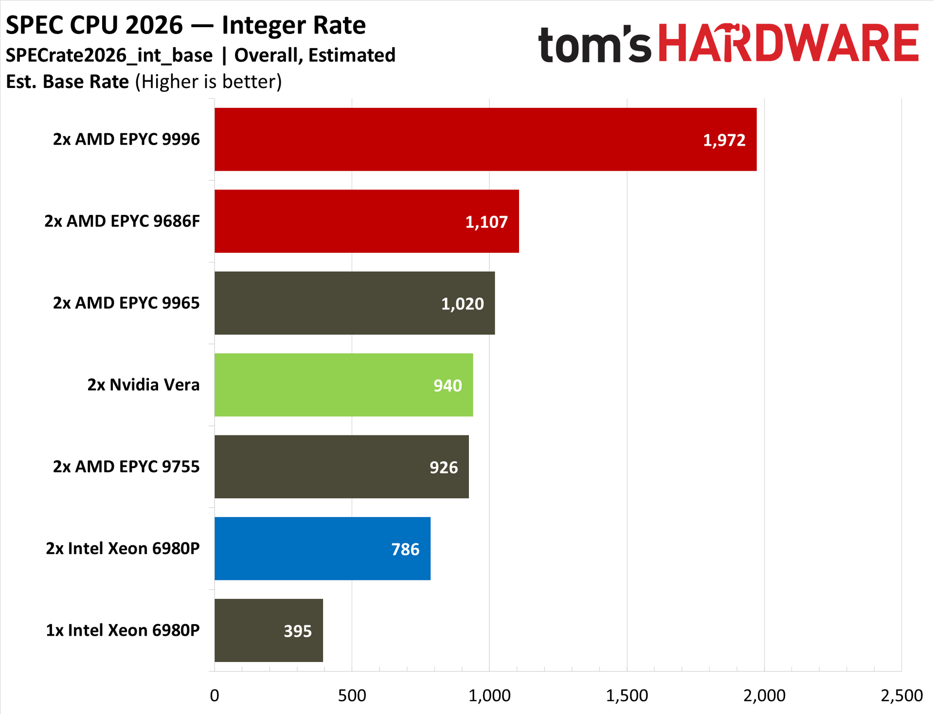
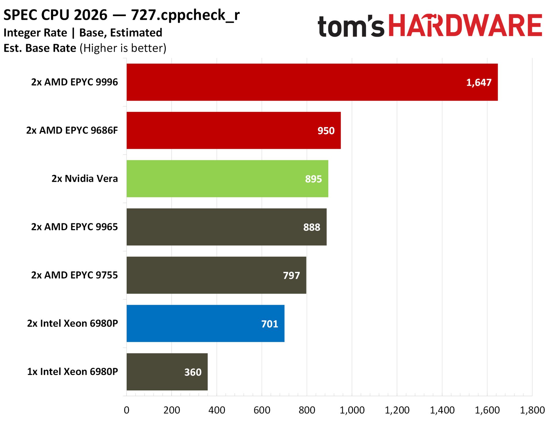
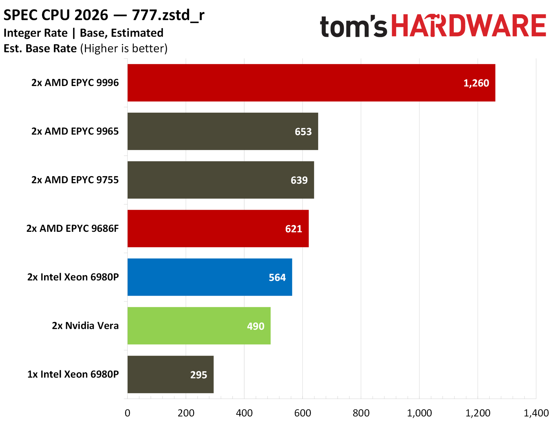
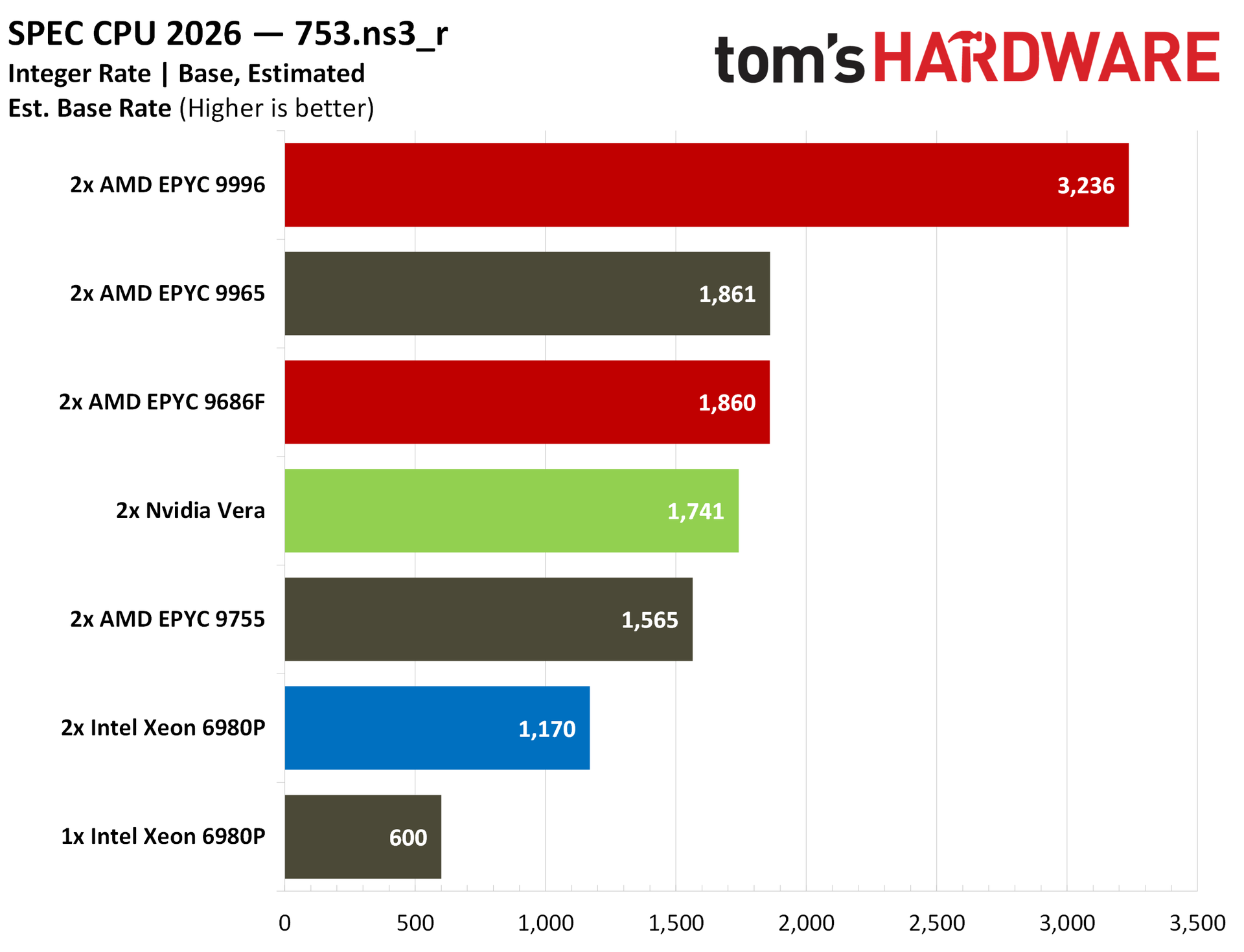
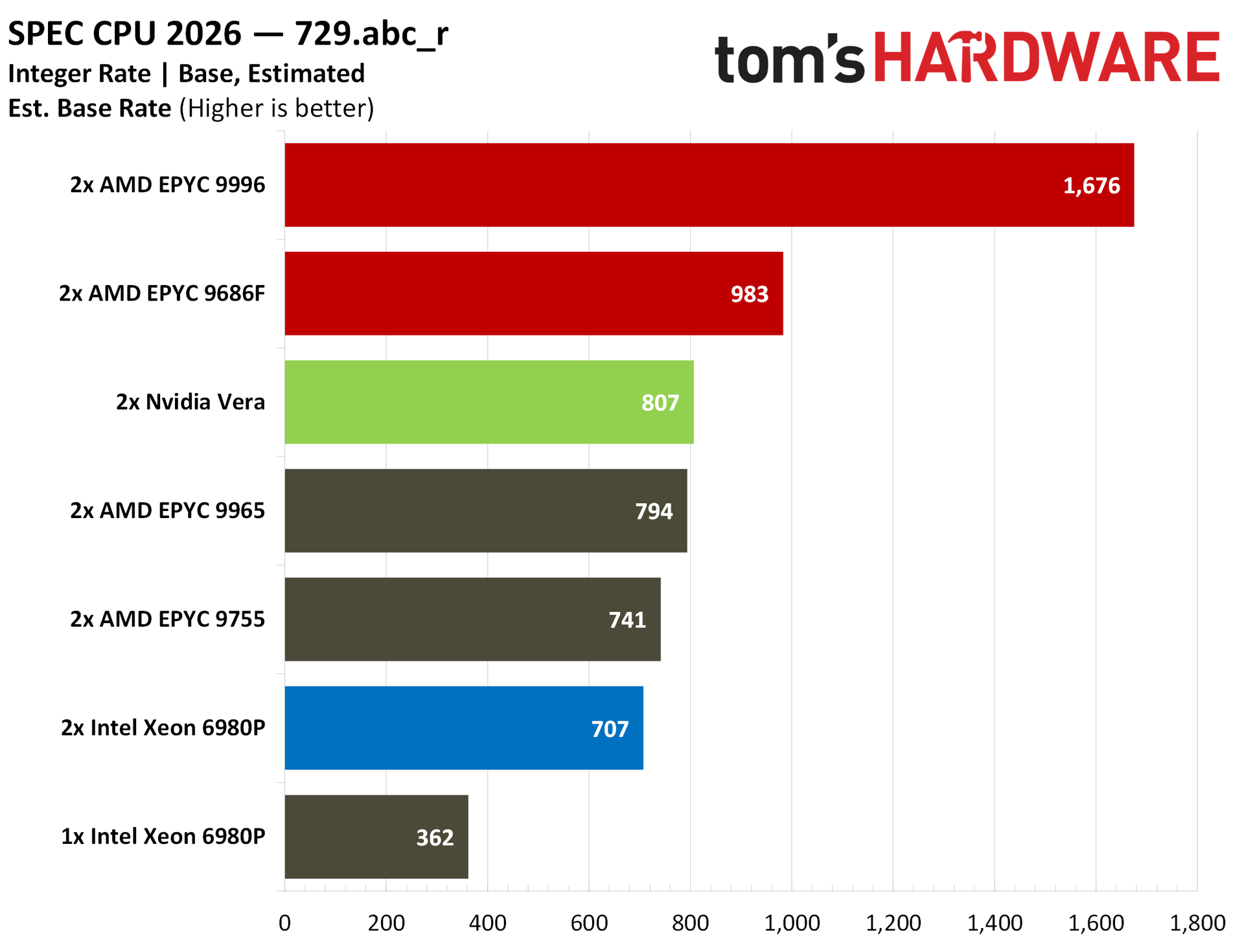
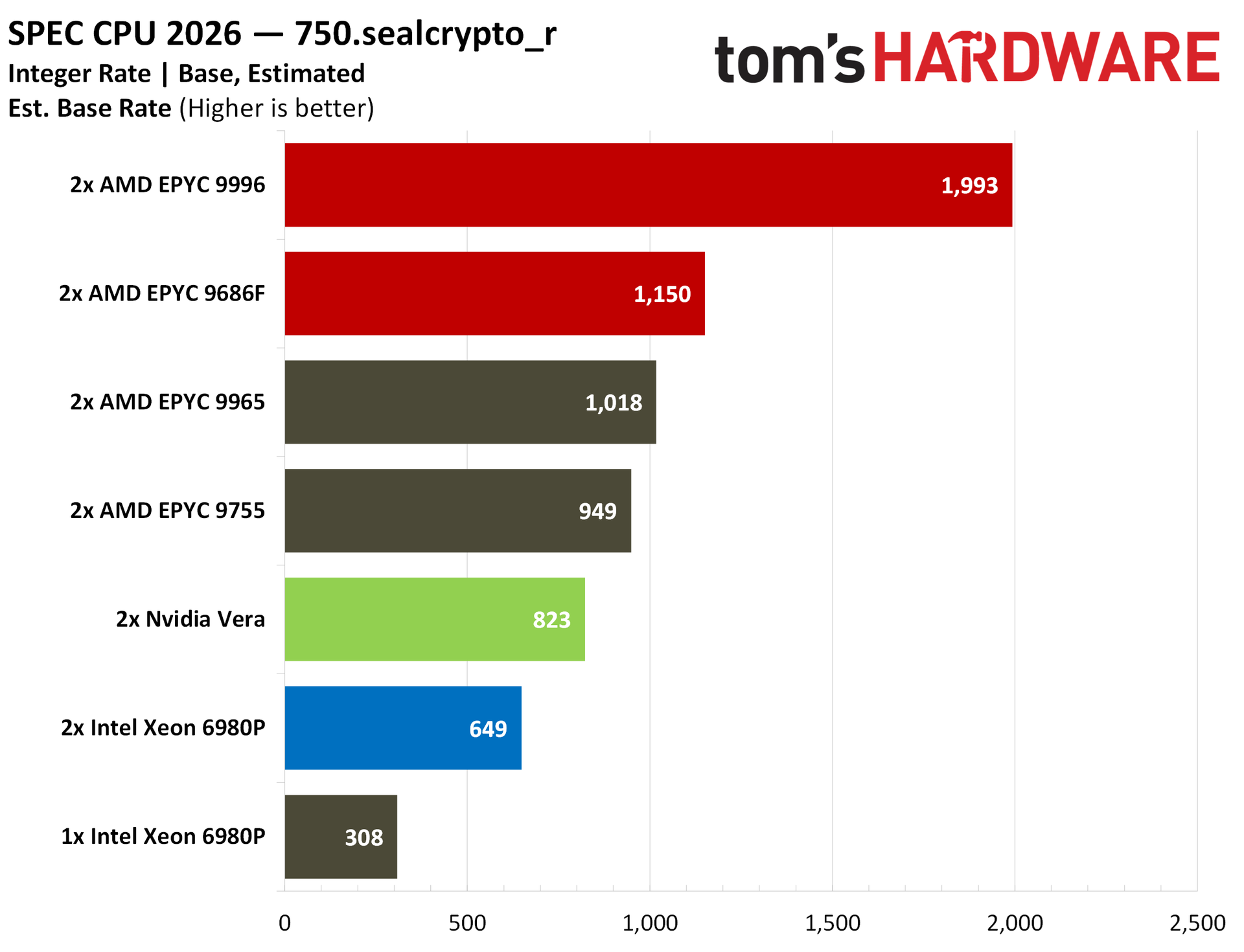
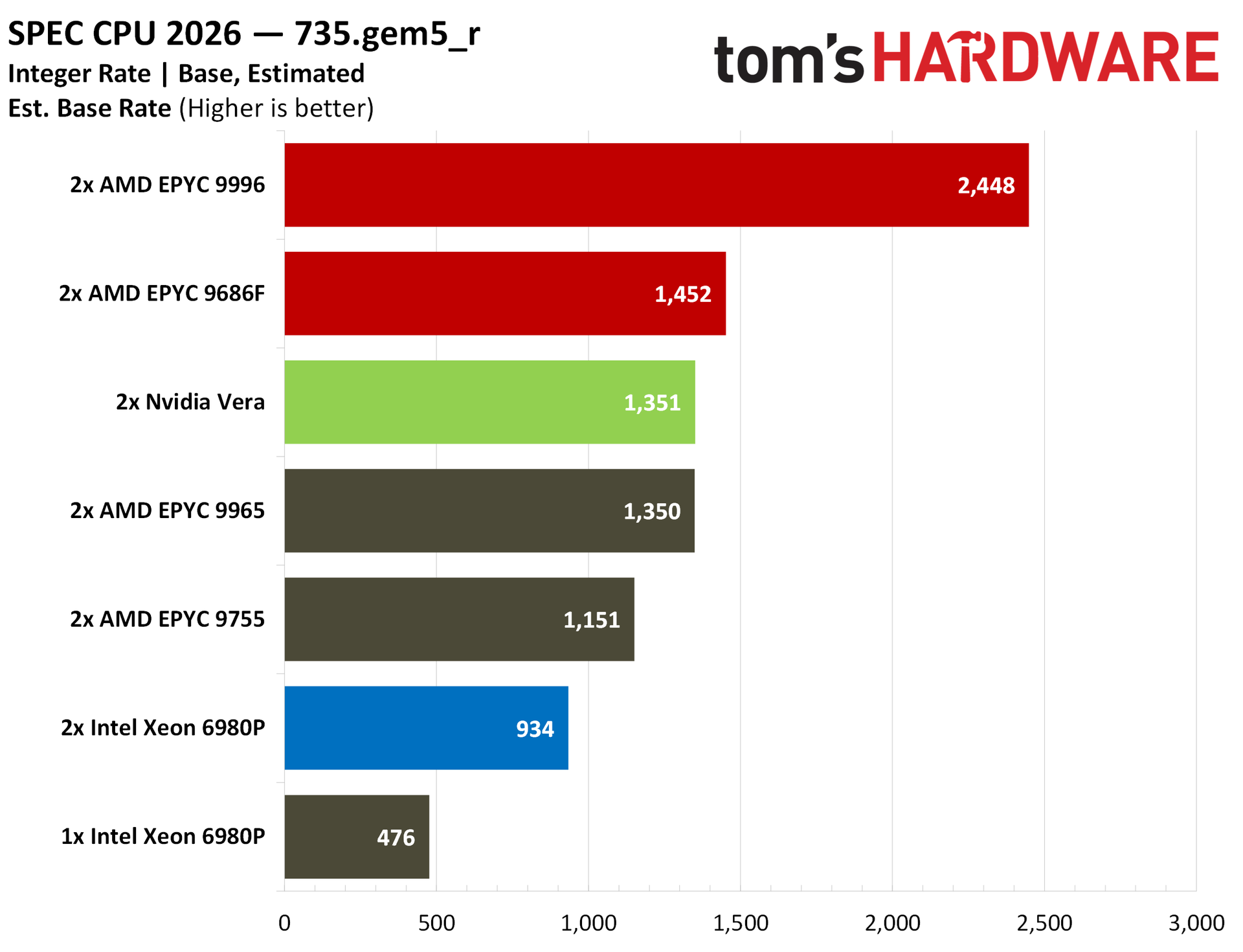
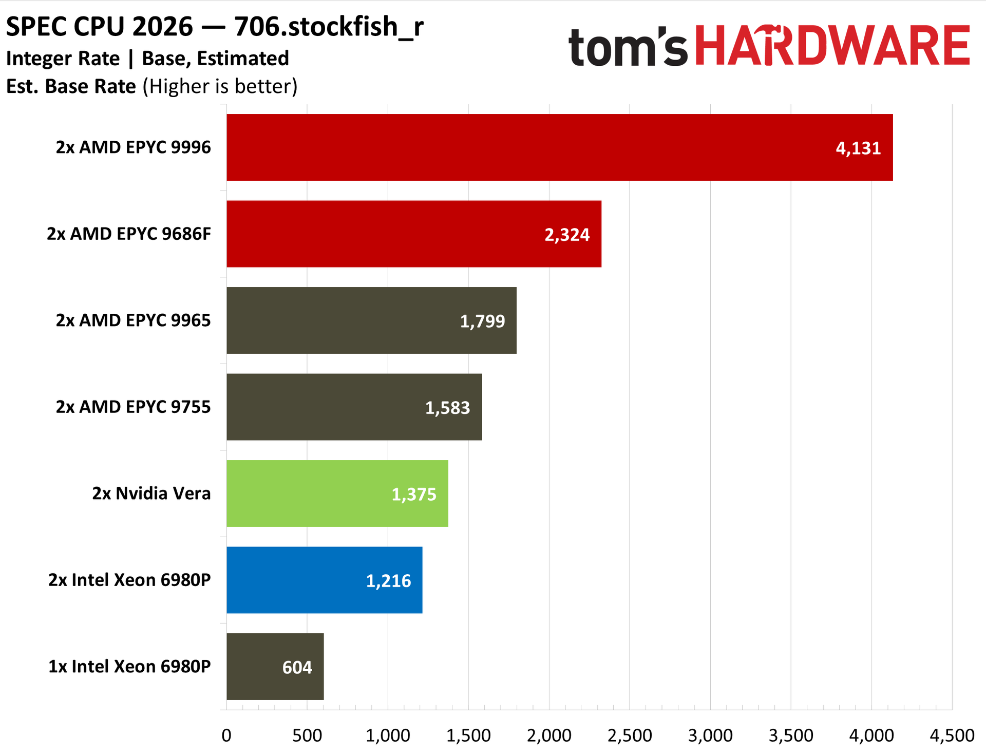
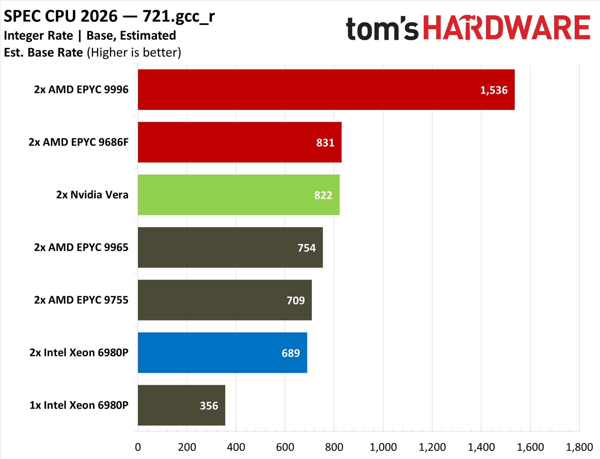
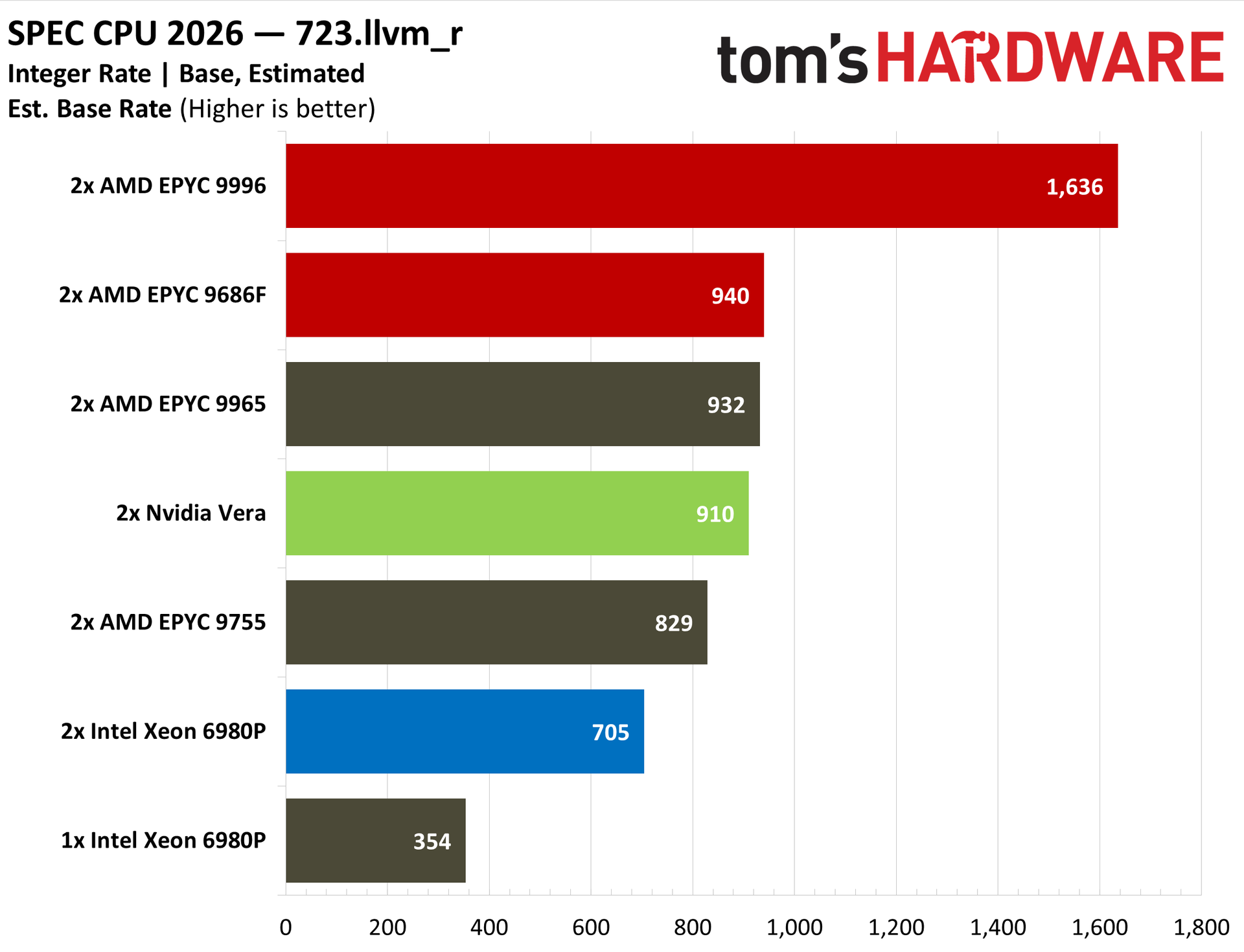
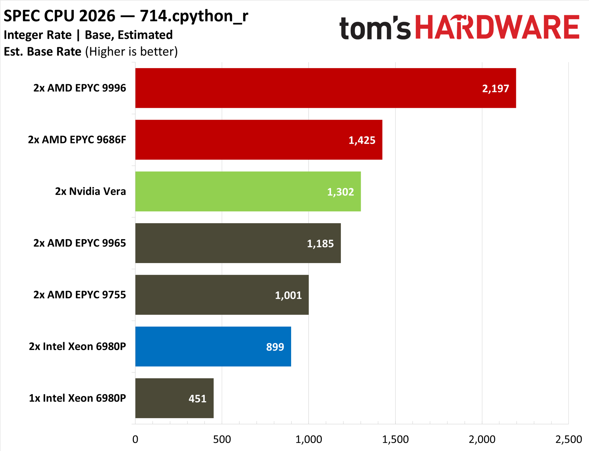
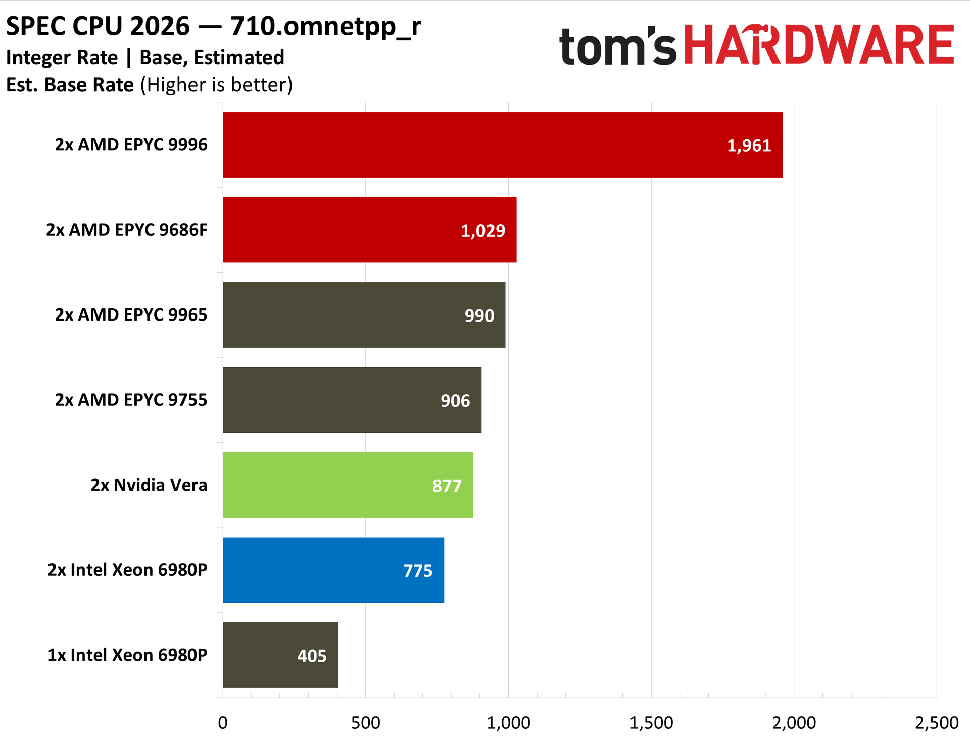
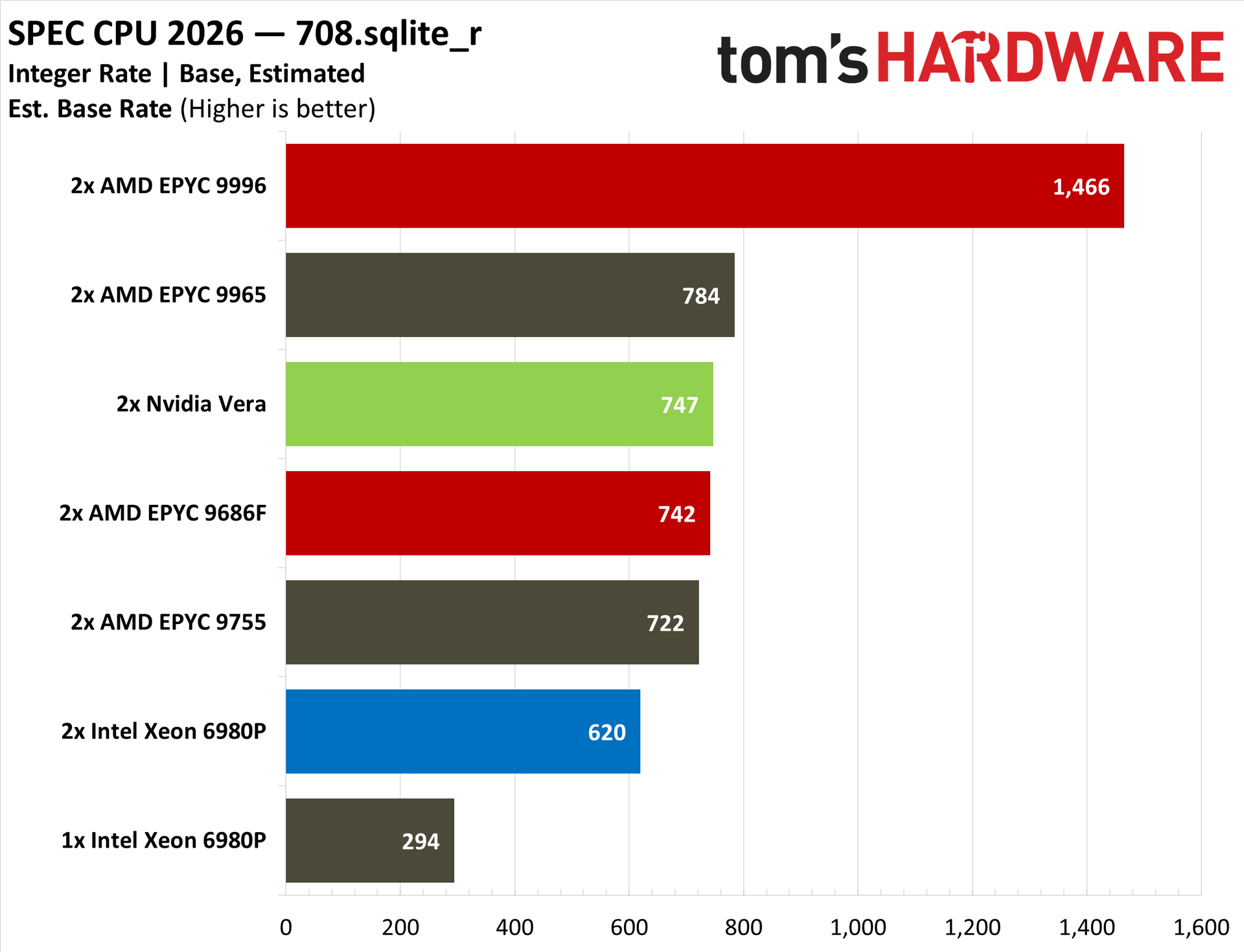
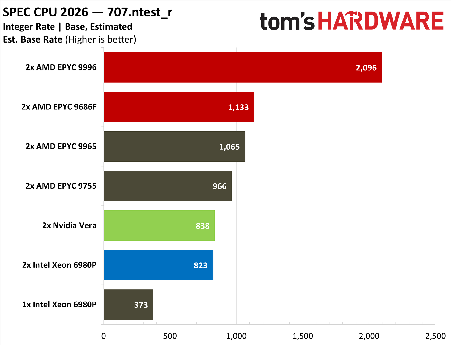
The overall intrate scores set the tone, particularly for the EPYC 9996. It has access to 1,024 threads in a 2P configuration, multiplying the clear speed improvements in Zen 6 broadly across more threads compared to last-gen’s top-end EPYC 9965. The 9996 scored a massive 93% higher in this test, though that number requires some context.
Both throughput benchmarks in SPEC reward not only how much work is done, but also how quickly it’s done. With access to a much larger thread pool and improvements in Zen 6 broadly, there’s that multiplicative effect when looking at pure throughput. A 2P EPYC 9996 system is 93% faster than a 2P EPYC 9965 system in this benchmark, but not broadly across the board.
The EPYC 9686F provides some context, which is still good news for AMD, just not on the level of doubling the performance of the previous generation. We unfortunately didn’t have access to a 9575F for a closer gen-on-gen comparison, but the EPYC 9755 is a decent proxy, with its 128 cores and relatively high 4.1 GHz boost clock. Compared with that CPU, the EPYC 9686F in a 2P configuration is 19% ahead — not too shabby considering the thread disadvantage.
Critically for AMD, the EPYC 9686F is also 17% ahead of Nvidia’s Vera CPU. Vera punches far above its weight class compared to the x86 competition, as evidenced by its matchup against the 9755 and Intel’s flagship Granite Rapids-AP 6980P.
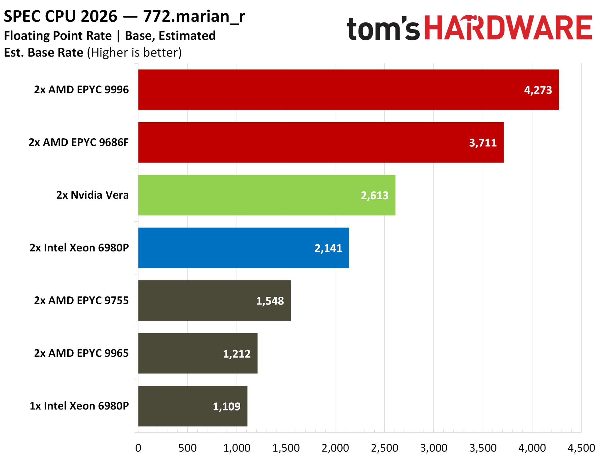
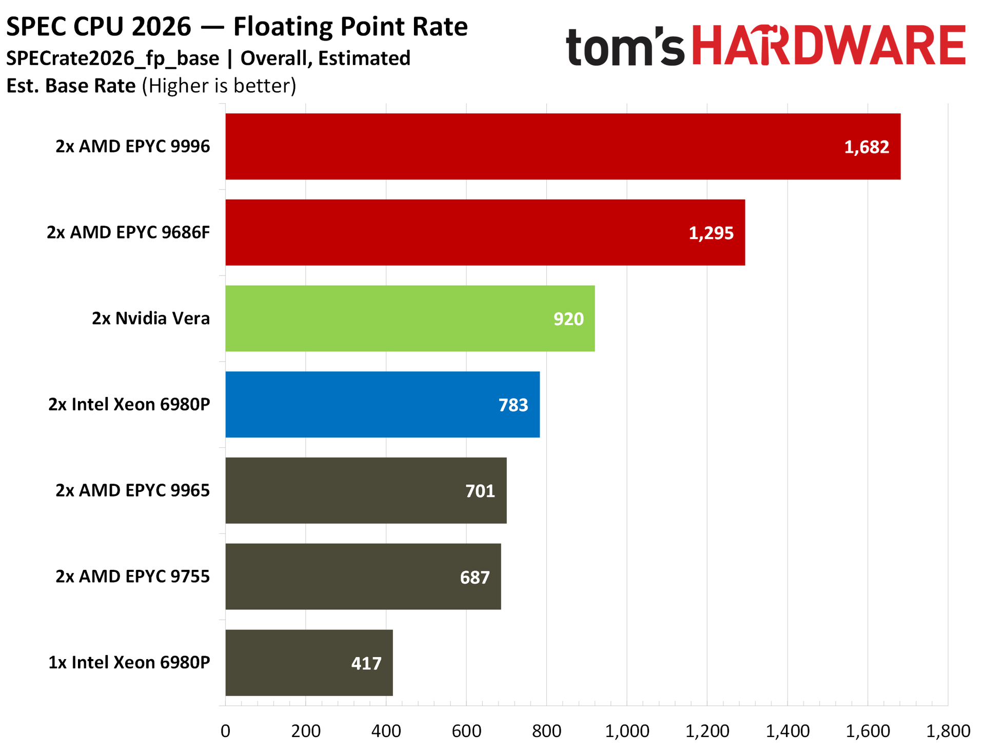
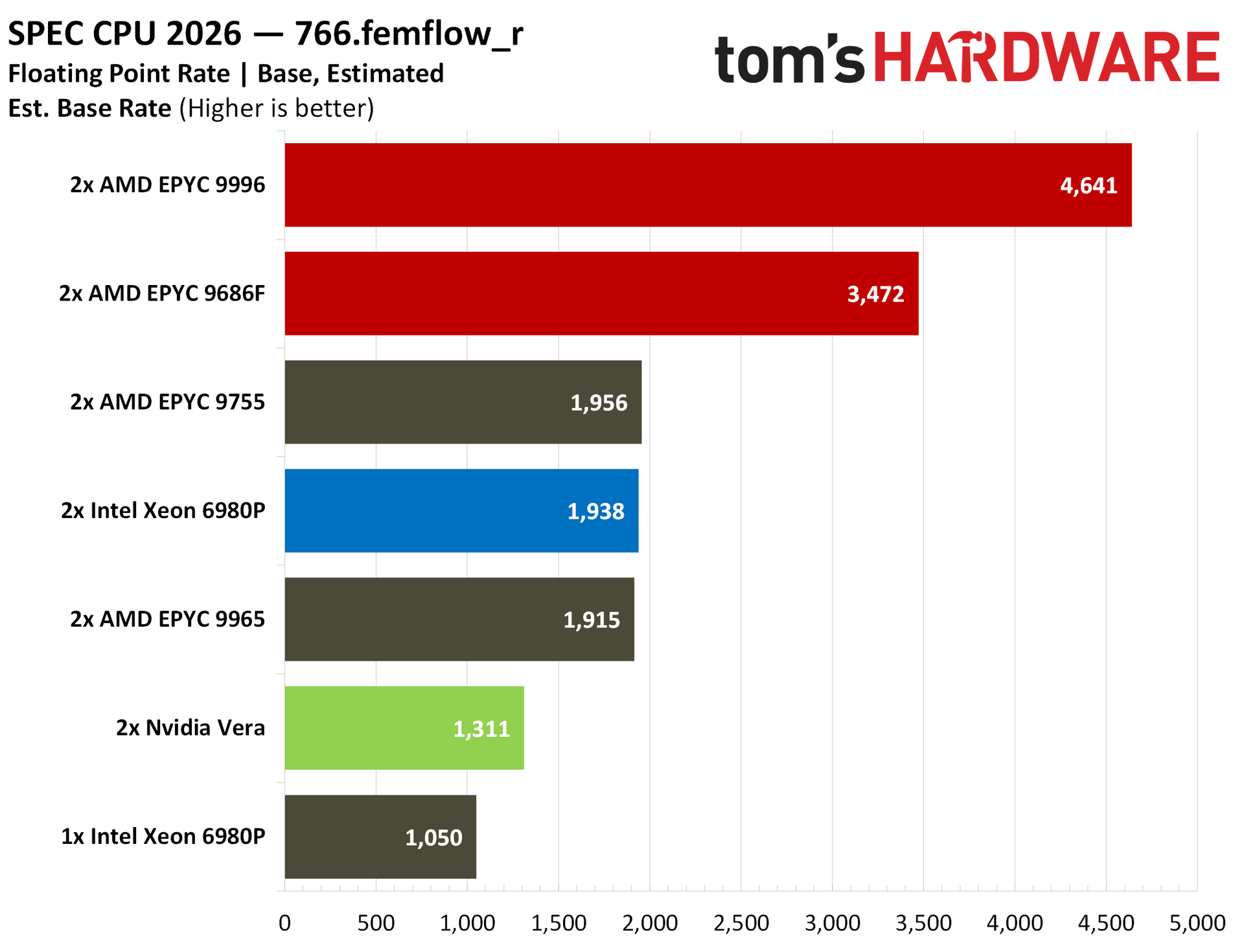
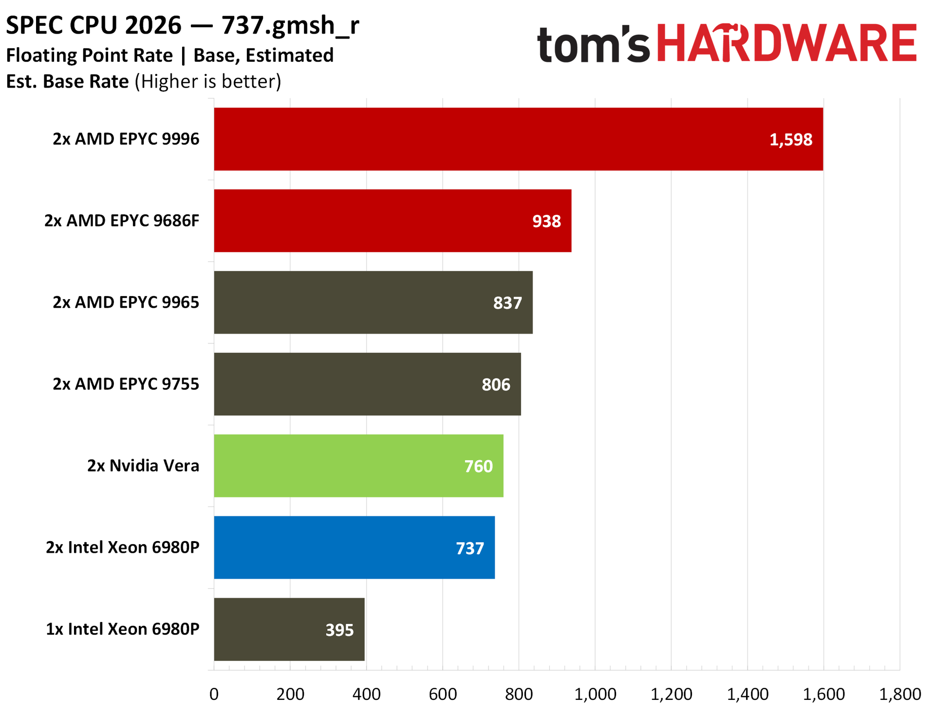
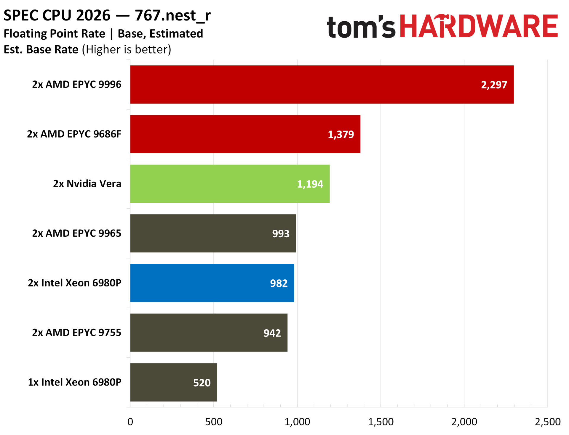
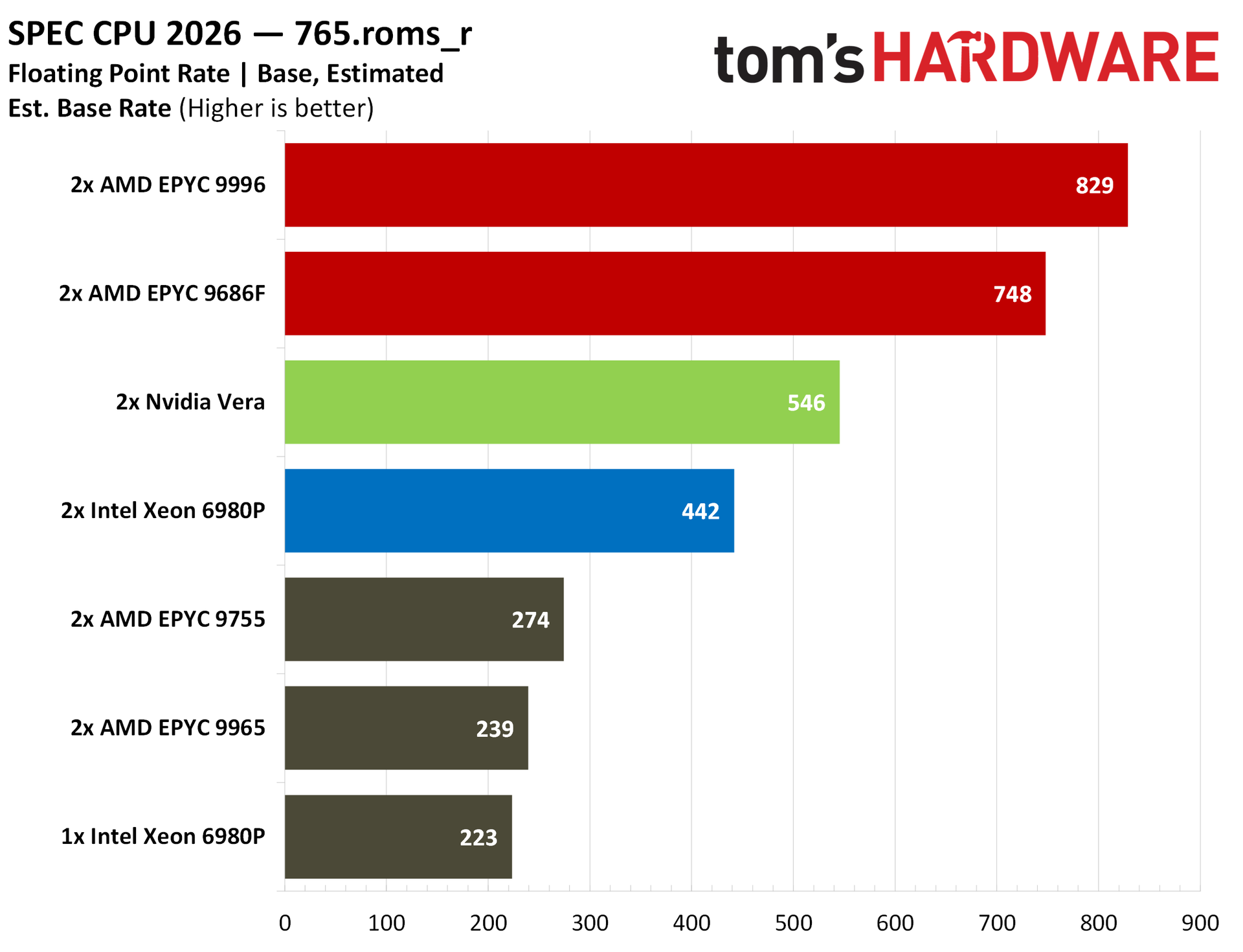
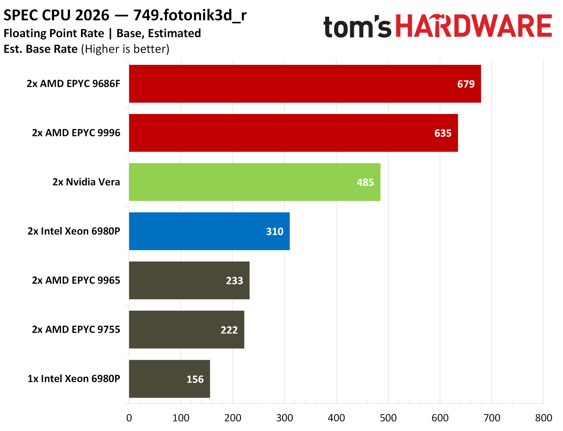
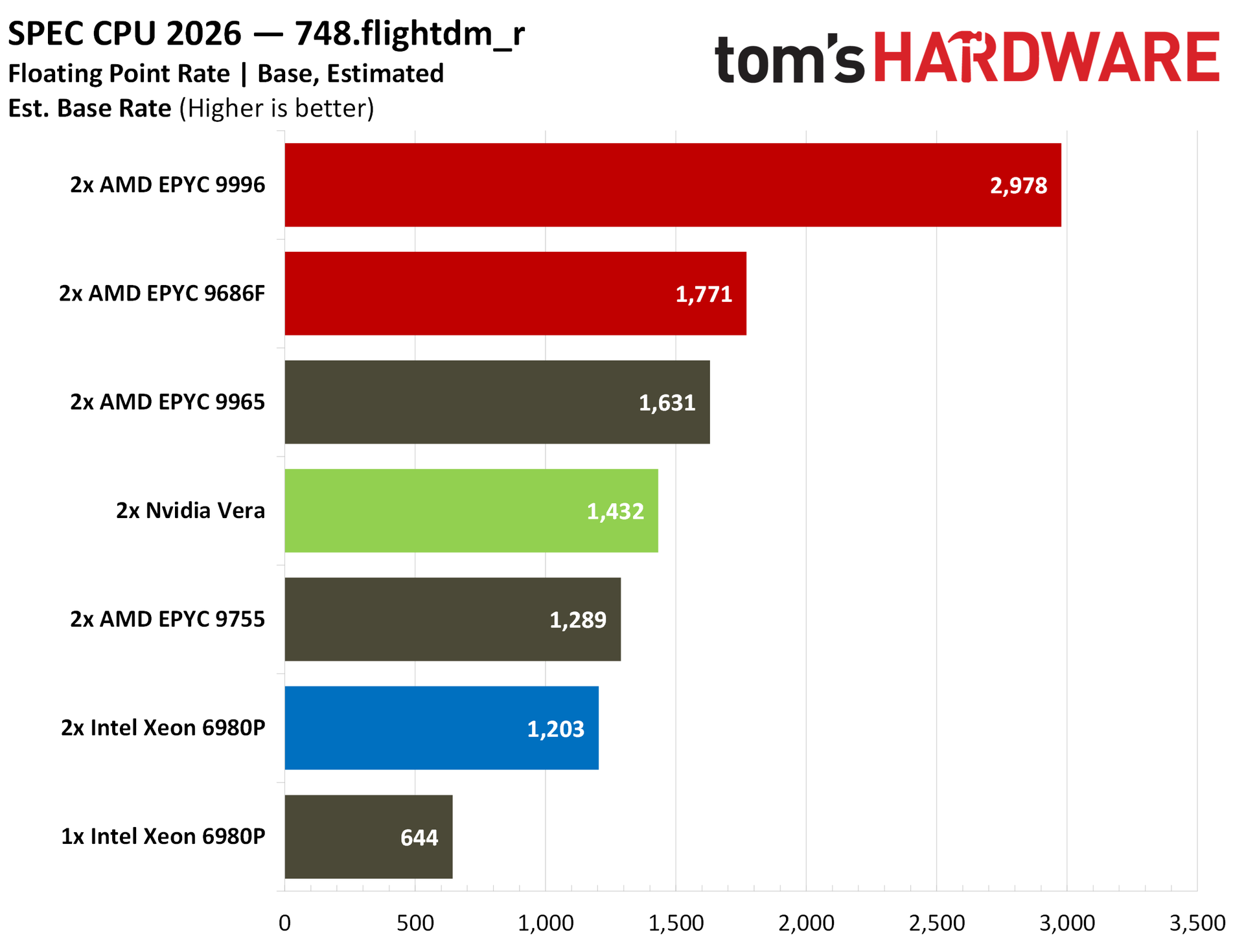
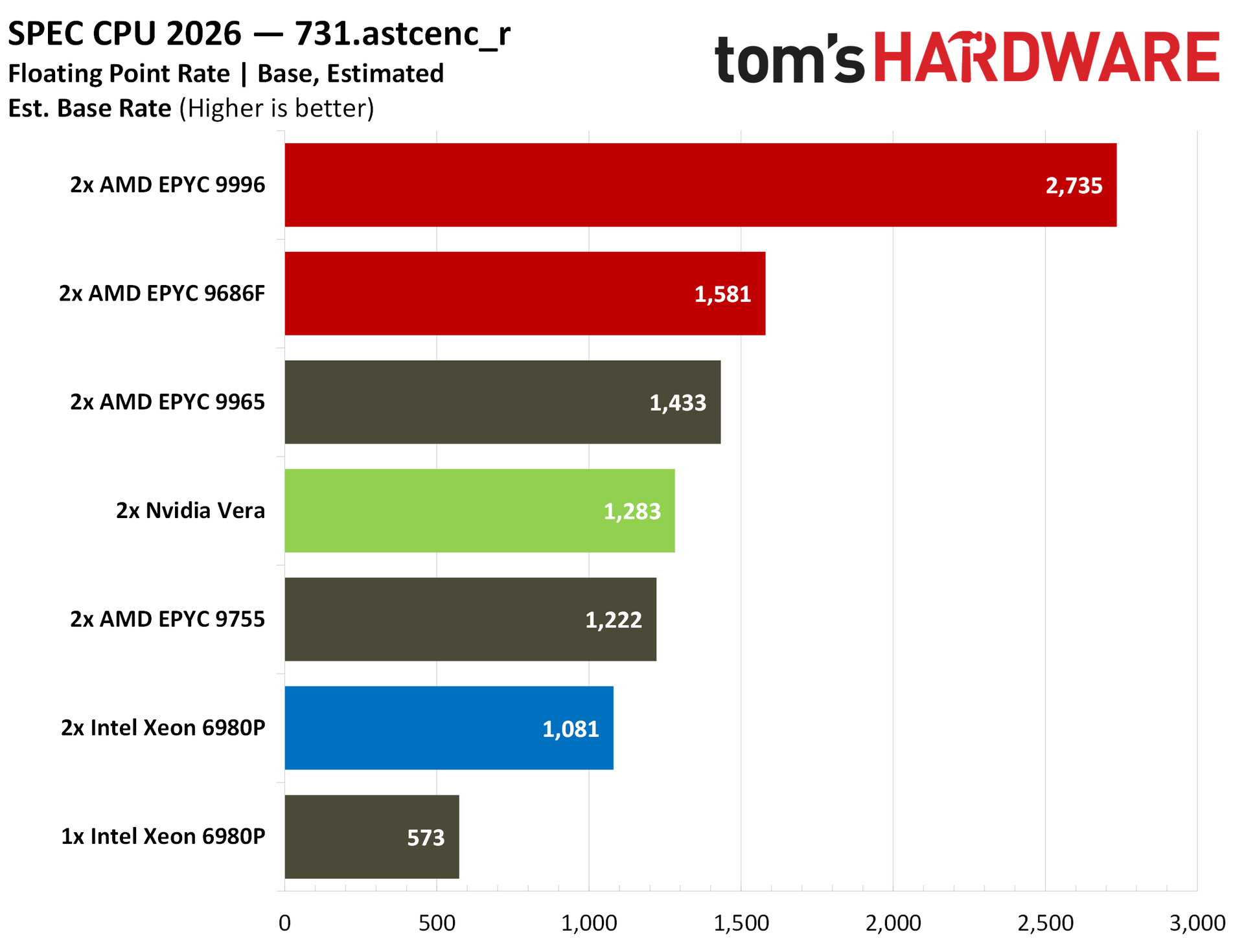
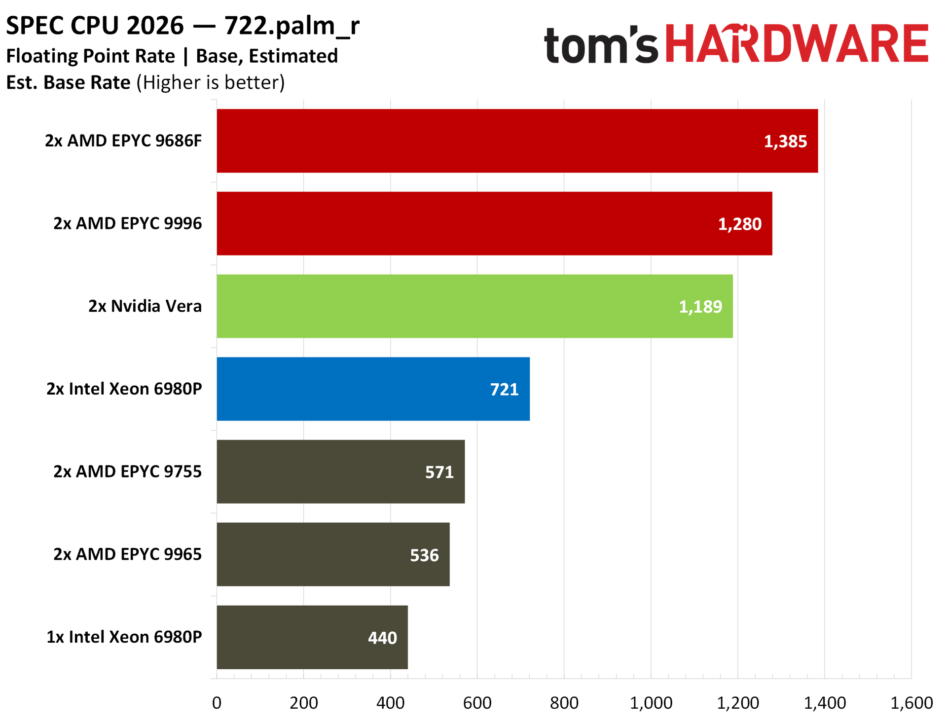
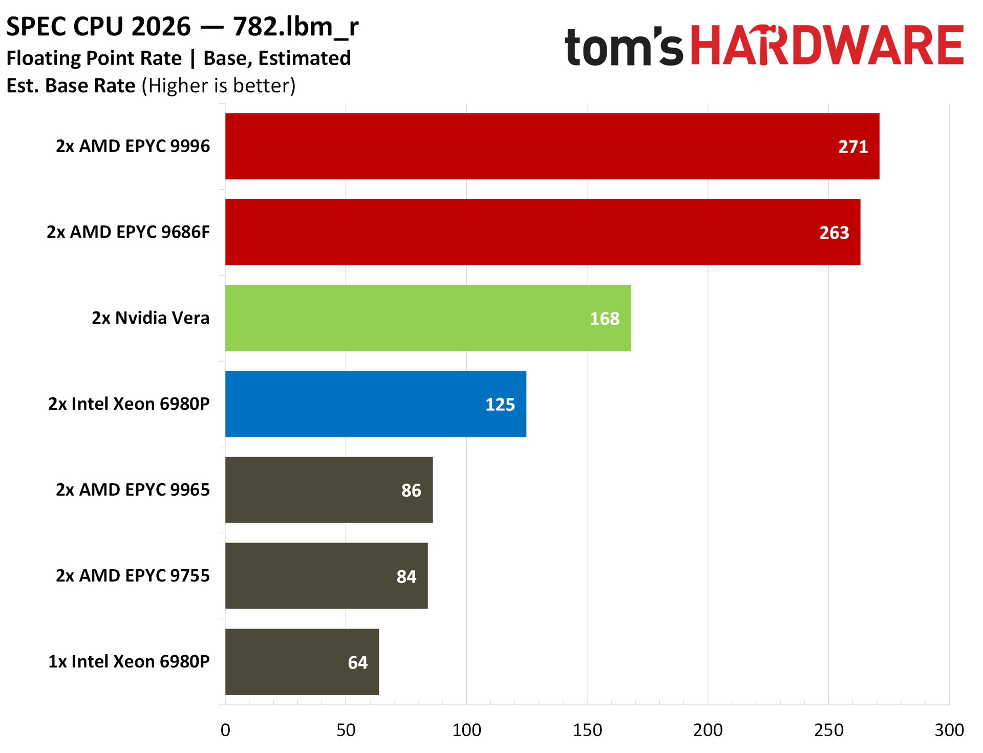
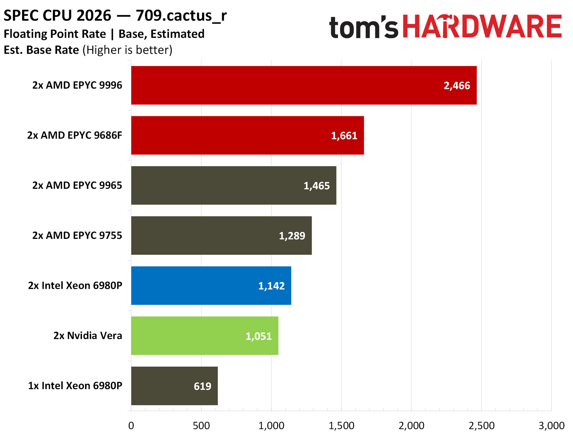
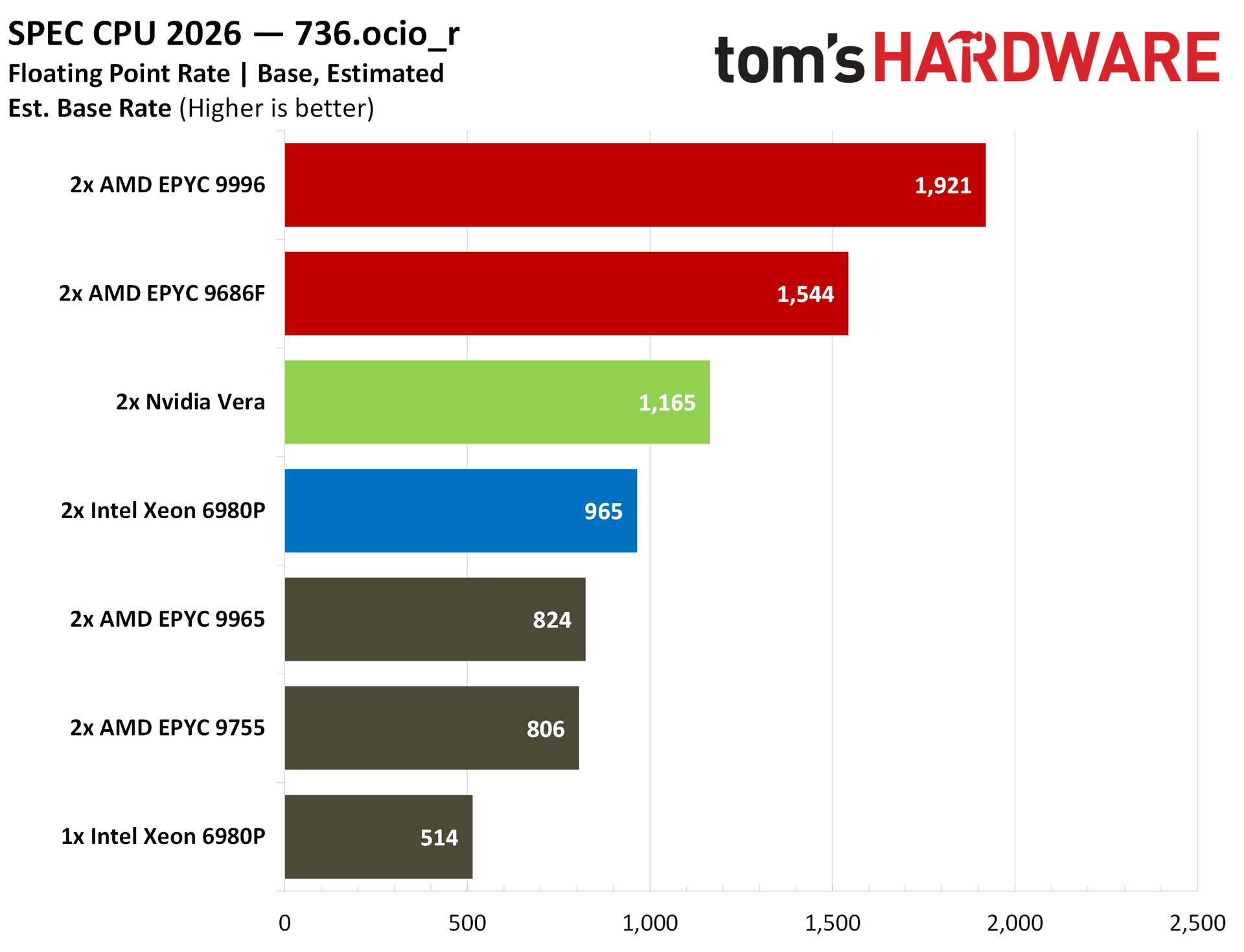
Flipping over to float performance, AMD did a lot of work on the vector engine in Zen 6, and it shows up in fprate. The differences between the EPYC 9996 and 9686F are smaller, though not in a way where both chips are hamstrung. Rather, the EPYC 9696F is able to push up closer to the 9996, leaving both Zen 6 chips running circles around the field.
AMD more than doubled the score with its Zen 6 chips compared to our Zen 5 touchpoints, which is a massive achievement. The EPYC 9686F excels even more over Vera in fprate with a 40% lead, despite only a minor bump in core count (88 on Vera to 96 on the 9686F). Intel’s Granite Rapids-AP isn’t in the conversation here for raw performance; though, apparently the range is still in high-enough demand that Intel has increased production in the tight CPU environment we’re currently experiencing.
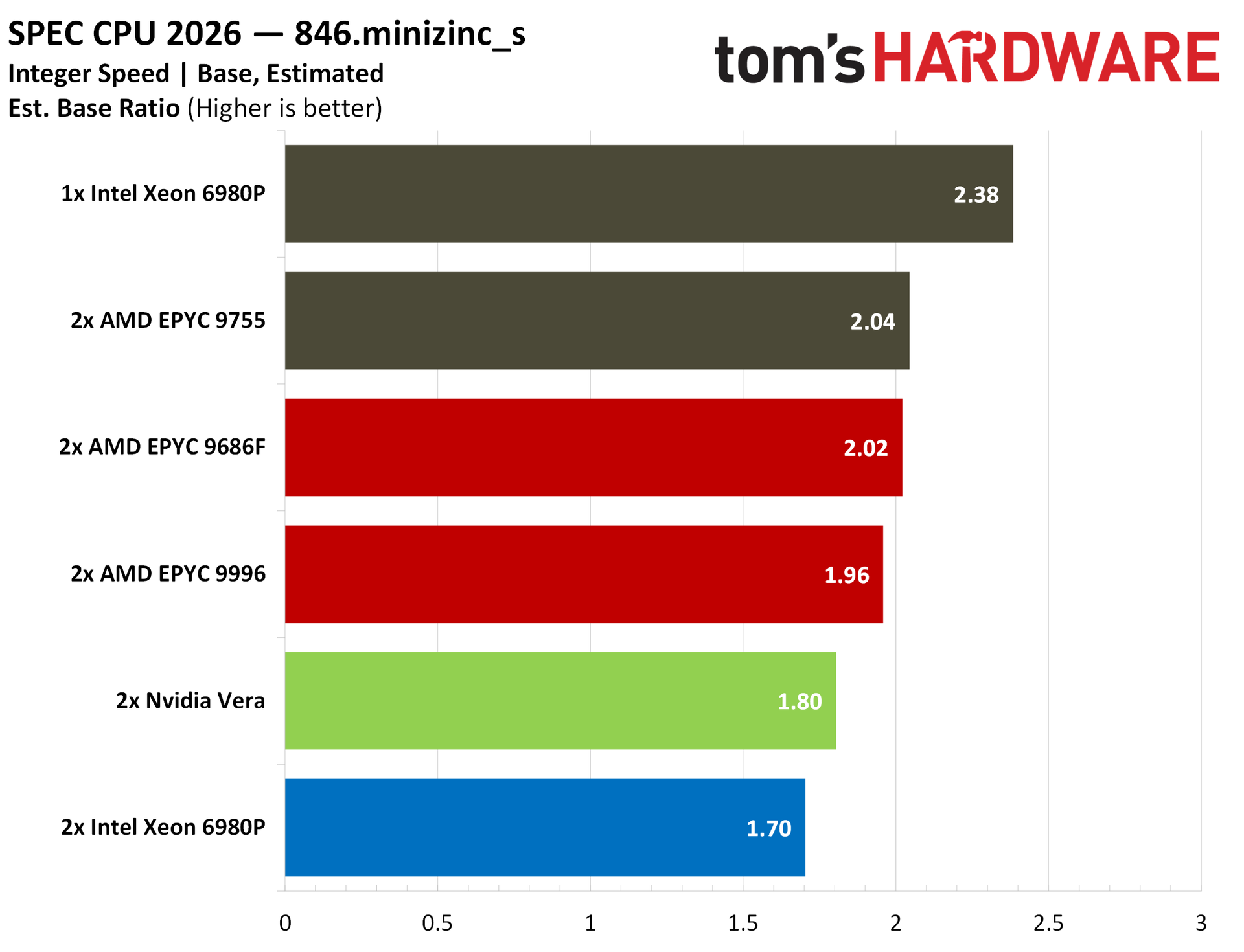
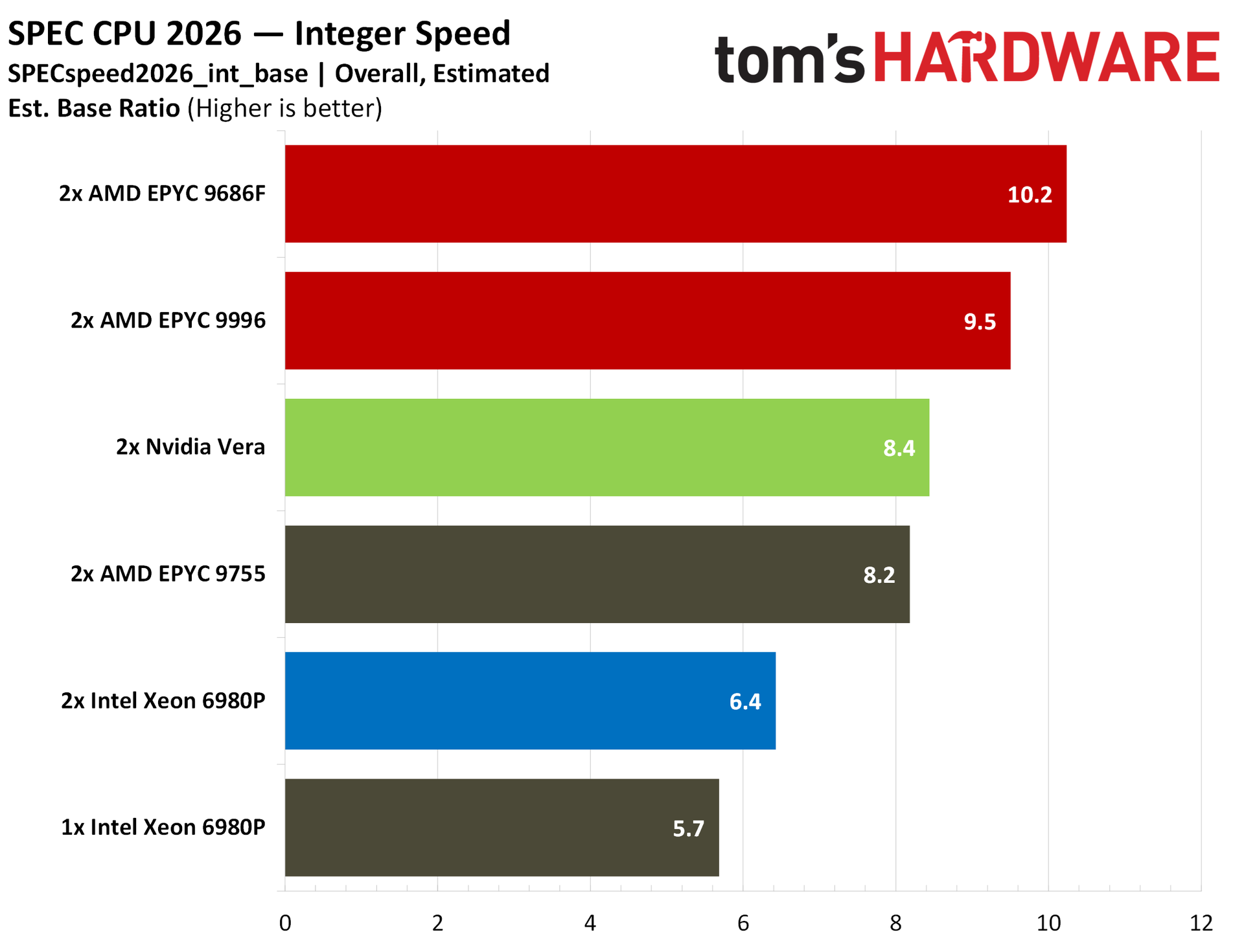
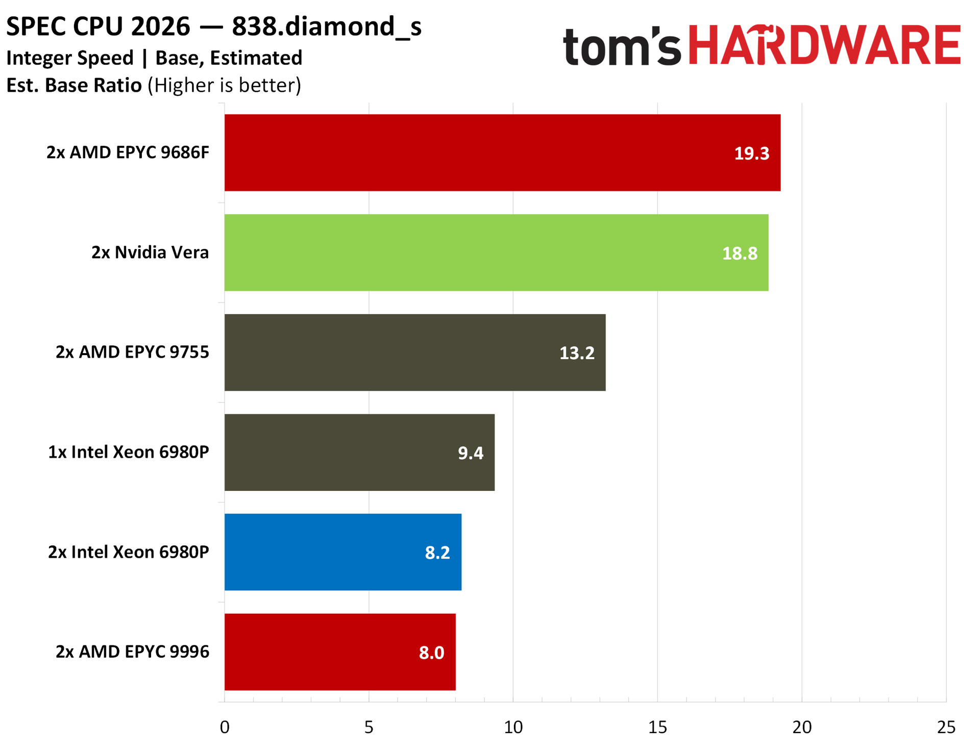
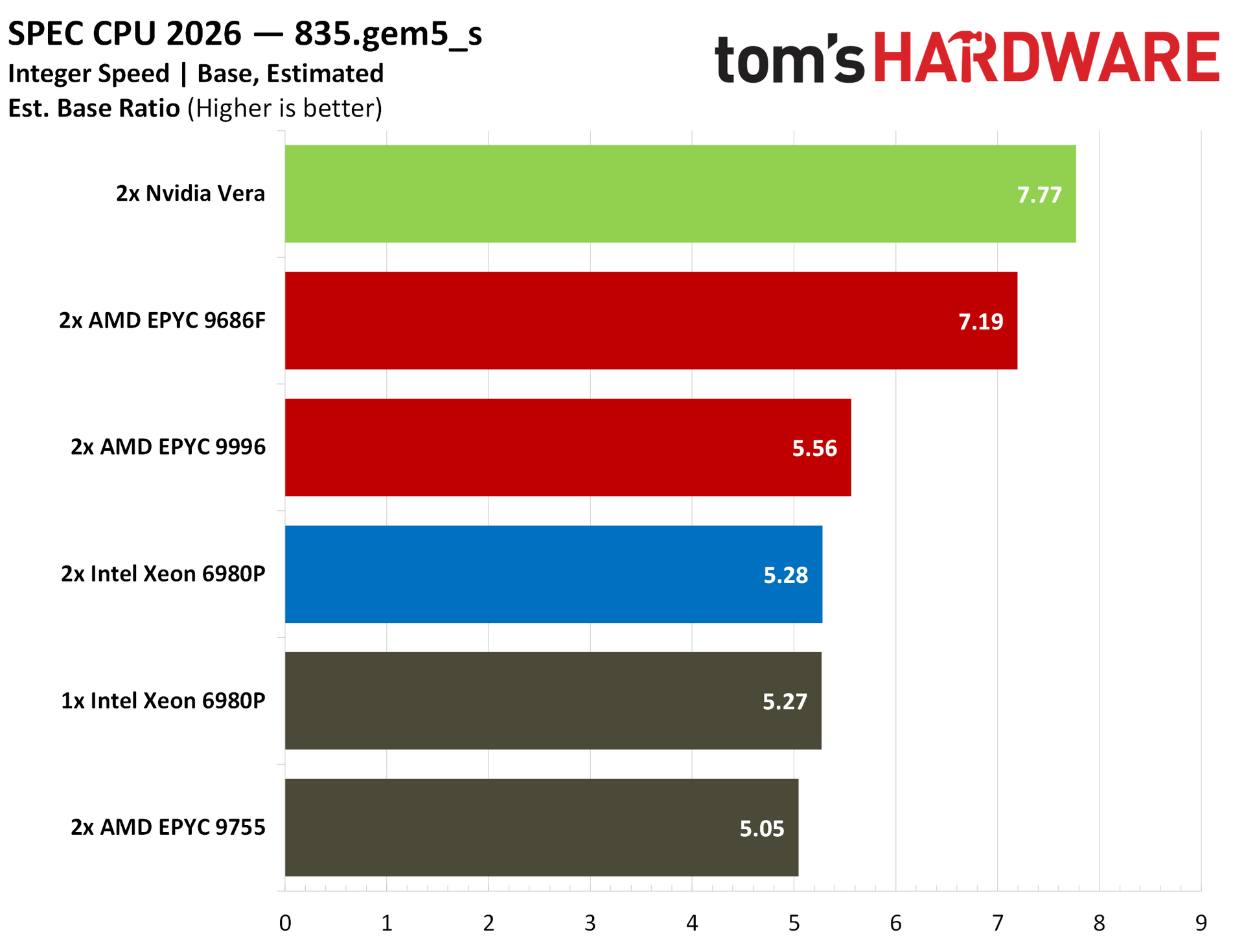
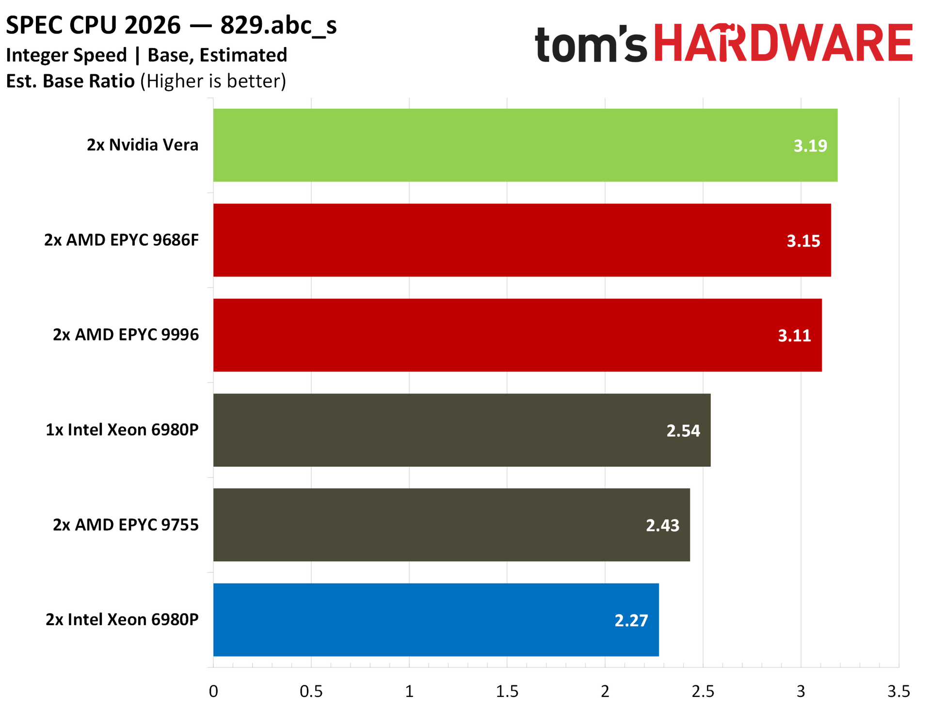
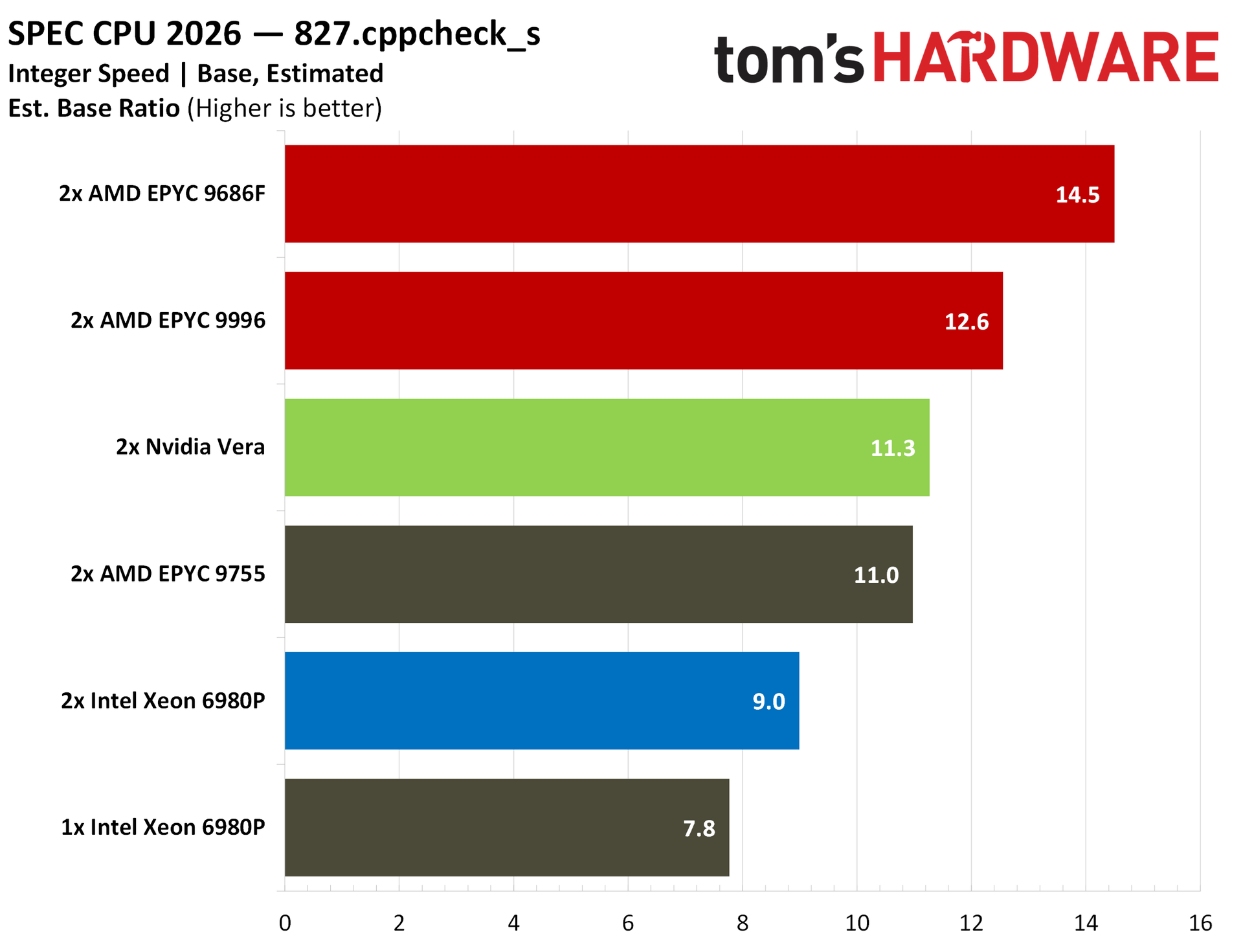
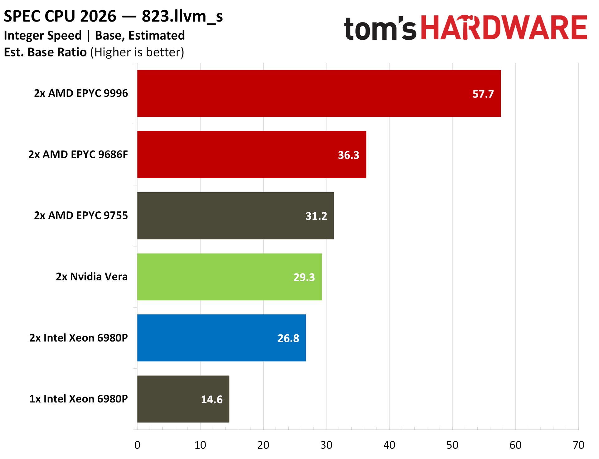
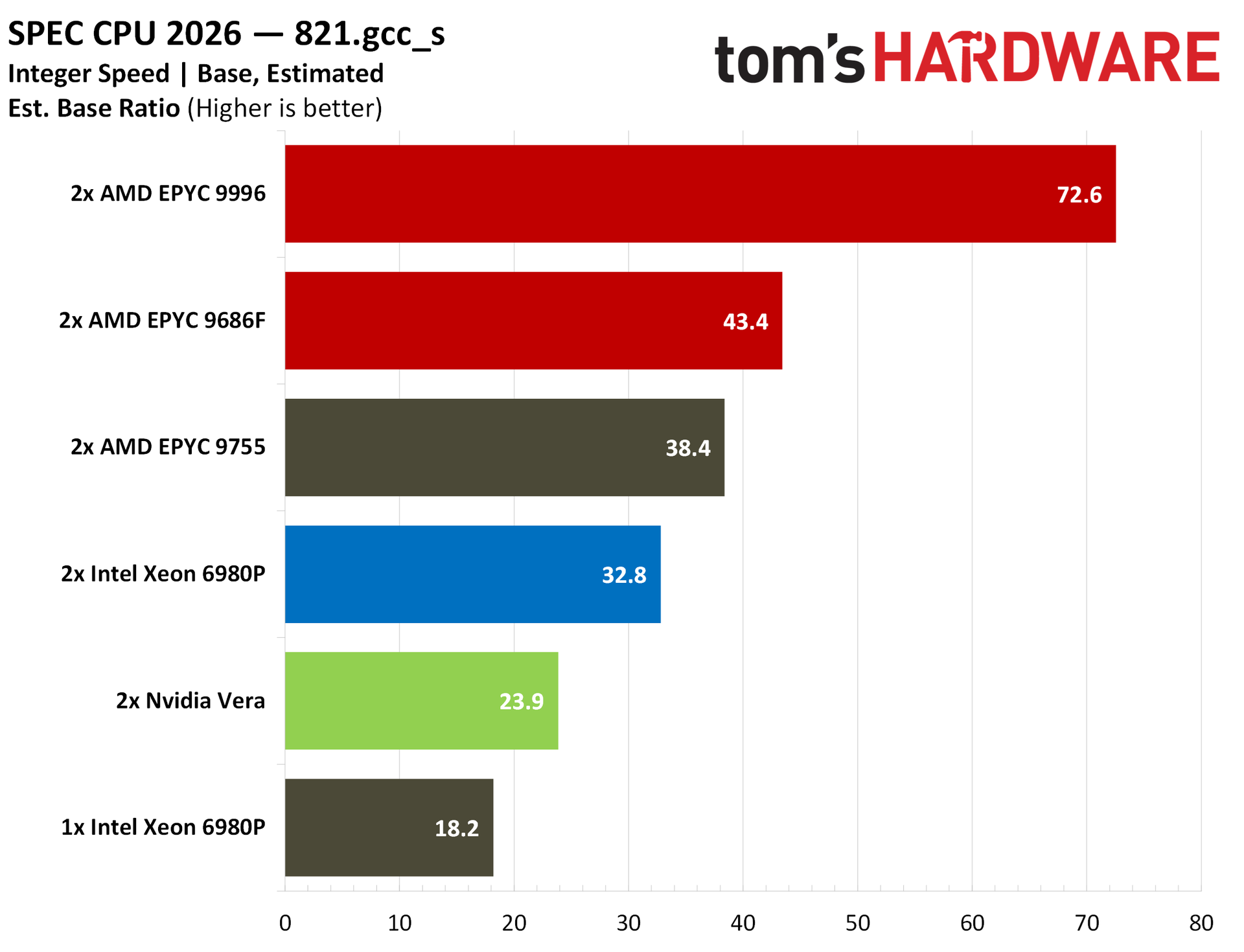
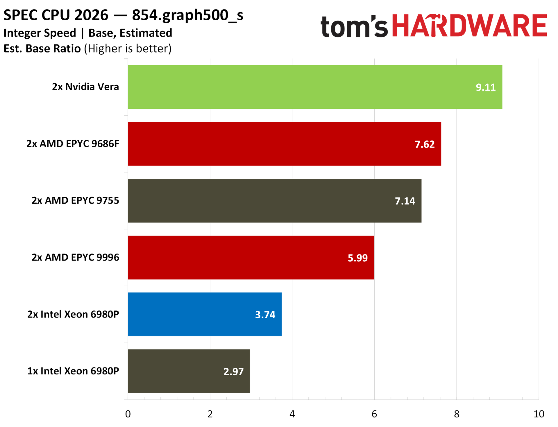
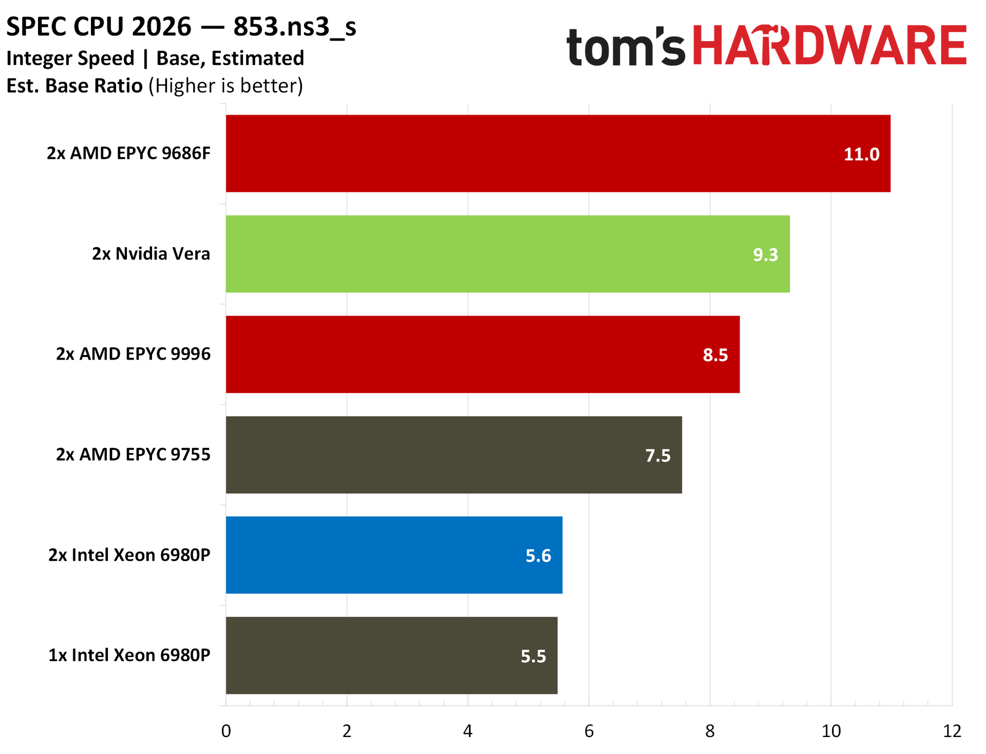
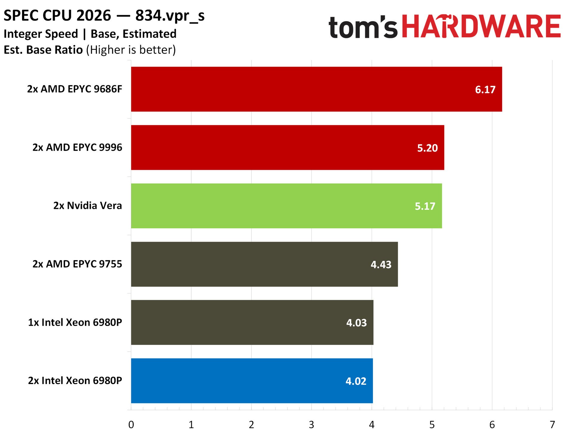
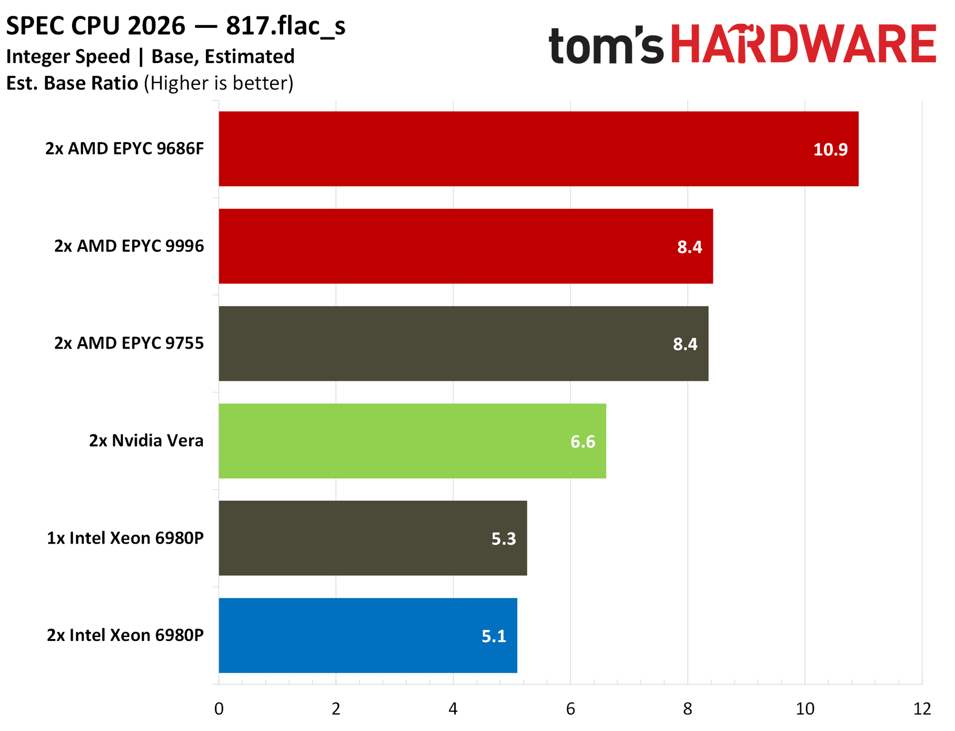
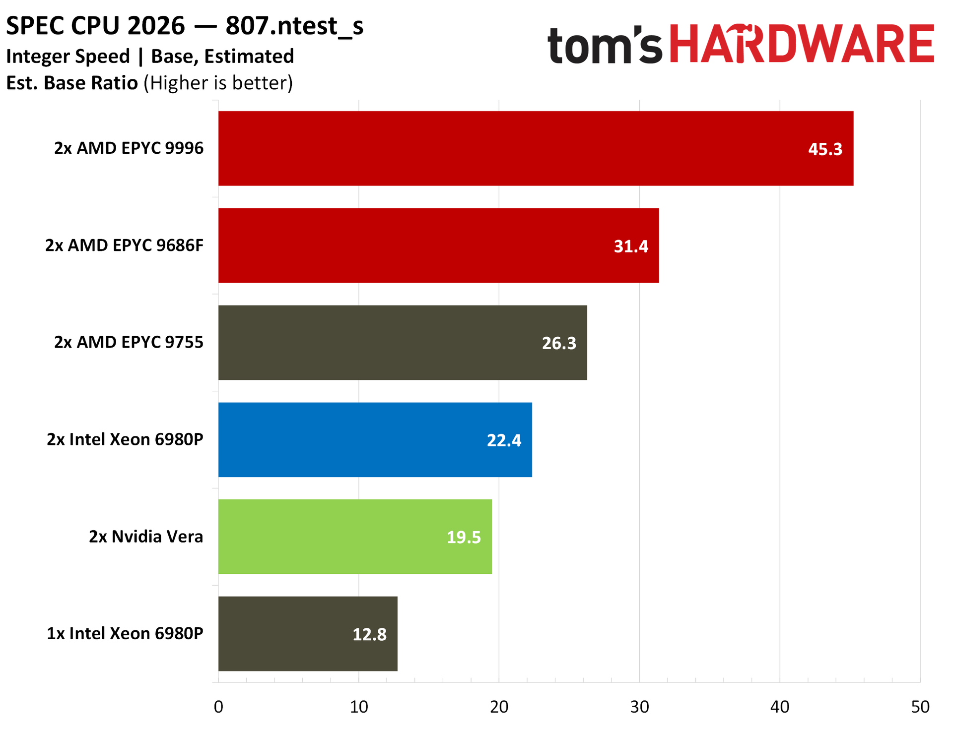
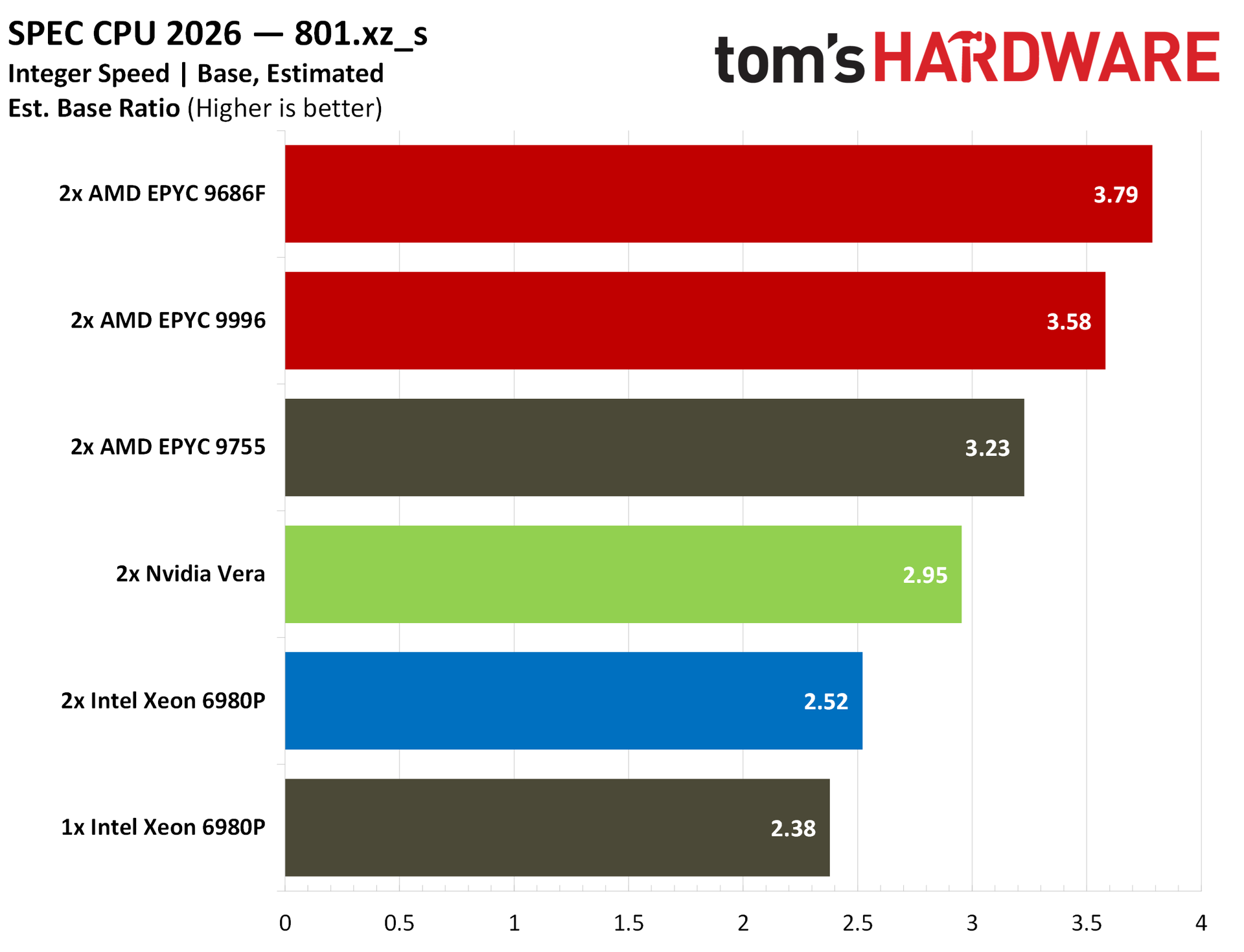
These throughput benchmarks are most representative of how these CPUs will actually be deployed, running multiple copies of applications under high concurrency. However, SPEC CPU also includes its speed suite, which looks at application performance when you can dedicate the whole chip to running just that one application, more along the lines of a client CPU benchmark.
The EPYC 9686F naturally looks better here with its blistering 5 GHz boost clock. In the integer suite, the frequency-optimized chip is 21% ahead of Vera, both in a 2P configuration. The 9996 still holds up, only falling short of the 9686F, despite much more inter-CCD communication.
SPEC shows the various improvements in Zen 6 showing up in a compounding fashion. There’s the new microarchitecture with an optimized vector path, but also more cores per CCD. And also support for higher memory speeds, as well as more memory channels. In isolation, any of these improvements are solid (if rote) for typical gen-on-gen improvements. Add them up in a workload that can take advantage of all of those improvements, however, and Zen 6 is blistering.
AMD Zen 6 EPYC ‘Venice’ 9996 and 9686F Python and memory benchmarks
AMD Zen 6 EPYC ‘Venice’ 9996 and 9686F Python and memory benchmarks
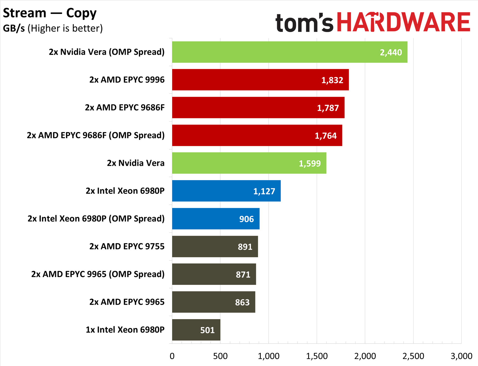
Two of the biggest performance vectors in the agentic era are memory performance and Python performance, at least at the moment. Agentic frameworks are largely defined by Python between LangGraph and CrewAI, though alternative frameworks written in TypeScript and Rust have started to appear as well. Regardless, Python remains important for agentic CPUs right now.
Similarly, memory bandwidth is important for certain types of agents, particularly those that need to query large databases, regardless of if they’re a traditional relational database written in SQL or a non-relational database.